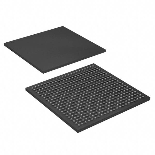
Viz Specifikace pro podrobnosti o produktu.

EP3SE50F484C4LN
Product Overview
- Category: Field Programmable Gate Array (FPGA)
- Use: EP3SE50F484C4LN is a high-performance FPGA designed for various applications in the electronics industry.
- Characteristics: This FPGA offers advanced features such as high-speed performance, low power consumption, and reconfigurability.
- Package: The EP3SE50F484C4LN comes in a 484-pin FineLine BGA package.
- Essence: It is a key component used to implement digital logic circuits and perform complex computations in electronic systems.
- Packaging/Quantity: The EP3SE50F484C4LN is typically sold individually or in small quantities.
Specifications
- Logic Elements: 49,152
- Embedded Memory: 2,088 Kbits
- Maximum User I/Os: 316
- Clock Management: PLLs and DLLs
- Operating Voltage: 1.2V
- Operating Temperature: -40°C to 100°C
- Package Dimensions: 23mm x 23mm
Detailed Pin Configuration
The EP3SE50F484C4LN has a total of 484 pins. These pins are divided into different categories, including:
- Power Supply Pins: VCCINT, VCCAUX, VCCIO, GND
- Configuration Pins: CONF_DONE, nCONFIG, nSTATUS
- Clock Pins: CLK0, CLK1, CLK2
- Input/Output Pins: IO0, IO1, IO2, ..., IO315
For a complete pin configuration diagram, please refer to the manufacturer's datasheet.
Functional Features
- High-speed performance: The EP3SE50F484C4LN operates at high clock frequencies, enabling rapid data processing.
- Low power consumption: This FPGA is designed to minimize power usage, making it suitable for battery-powered devices.
- Reconfigurability: The EP3SE50F484C4LN can be reprogrammed to adapt to changing requirements, providing flexibility in system design.
Advantages and Disadvantages
Advantages
- Versatile: The EP3SE50F484C4LN can be used in a wide range of applications due to its high-performance capabilities.
- Scalable: It offers scalability, allowing users to choose the appropriate FPGA size based on their specific needs.
- Cost-effective: Compared to custom ASICs, FPGAs like the EP3SE50F484C4LN offer a more affordable solution for complex digital designs.
Disadvantages
- Complexity: Working with FPGAs requires expertise in digital design and programming, which may pose a challenge for beginners.
- Limited resources: The EP3SE50F484C4LN has a finite number of logic elements and memory, which may restrict the complexity of designs.
Working Principles
The EP3SE50F484C4LN utilizes programmable logic blocks and interconnects to implement digital circuits. These logic blocks consist of look-up tables (LUTs), flip-flops, and other components that can be configured to perform various functions. The interconnects allow for the routing of signals between different logic blocks, enabling the creation of complex circuitry.
The FPGA's configuration memory stores the user-defined logic and interconnect configurations. During operation, the FPGA reads this configuration data and dynamically reprograms itself to execute the desired functionality.
Detailed Application Field Plans
The EP3SE50F484C4LN finds applications in various fields, including:
- Communications: Used in networking equipment, routers, and switches to handle high-speed data processing and protocol conversions.
- Industrial Automation: Employed in control systems, robotics, and machine vision applications to perform real-time data processing and control tasks.
- Aerospace and Defense: Utilized in radar systems, avionics, and military-grade communication equipment for high-performance signal processing and encryption.
- Medical Devices: Integrated into medical imaging systems, patient monitoring devices, and diagnostic equipment to process and analyze medical data.
- Automotive: Used in advanced driver-assistance systems (ADAS), infotainment systems, and engine control units (ECUs) for efficient data processing and control.
Detailed and Complete Alternative Models
- EP3C16F484C6N
- EP4CE115F29C7N
- EP2SGX90FF1508C4N
- EP1S30F780C6N
- EP4CE22F17C6N
These alternative models offer different combinations of logic elements, memory, I/Os, and other features, providing options for various project requirements.
*Note: The content provided above is a sample entry and may not reflect the actual specifications or details of the EP3SE50F484
Seznam 10 běžných otázek a odpovědí souvisejících s aplikací EP3SE50F484C4LN v technických řešeních
Sure! Here are 10 common questions and answers related to the application of EP3SE50F484C4LN in technical solutions:
Q: What is EP3SE50F484C4LN? A: EP3SE50F484C4LN is a specific model of Field-Programmable Gate Array (FPGA) manufactured by Intel.
Q: What are the key features of EP3SE50F484C4LN? A: Some key features of EP3SE50F484C4LN include 50,000 logic elements, 484-pin package, and support for various I/O standards.
Q: What are the typical applications of EP3SE50F484C4LN? A: EP3SE50F484C4LN can be used in a wide range of applications such as industrial automation, telecommunications, automotive systems, and high-performance computing.
Q: How can EP3SE50F484C4LN be programmed? A: EP3SE50F484C4LN can be programmed using hardware description languages (HDLs) like VHDL or Verilog, and then configured using programming tools provided by Intel.
Q: Can EP3SE50F484C4LN be used for real-time signal processing? A: Yes, EP3SE50F484C4LN is capable of real-time signal processing due to its high-speed performance and parallel processing capabilities.
Q: Does EP3SE50F484C4LN support communication protocols? A: Yes, EP3SE50F484C4LN supports various communication protocols such as UART, SPI, I2C, Ethernet, and PCIe.
Q: Can EP3SE50F484C4LN interface with external memory devices? A: Yes, EP3SE50F484C4LN has dedicated memory controllers that allow it to interface with external memory devices like DDR SDRAM or Flash memory.
Q: What are the power requirements for EP3SE50F484C4LN? A: EP3SE50F484C4LN typically operates at a voltage range of 1.2V to 3.3V, depending on the specific configuration and I/O standards used.
Q: Is EP3SE50F484C4LN suitable for low-power applications? A: While EP3SE50F484C4LN is not specifically designed for low-power applications, it does offer power-saving features like clock gating and dynamic power management.
Q: Are there any development boards available for EP3SE50F484C4LN? A: Yes, Intel provides development boards like the Cyclone III Starter Kit, which can be used for prototyping and testing solutions based on EP3SE50F484C4LN.
Please note that the answers provided here are general and may vary depending on the specific requirements and use cases.

