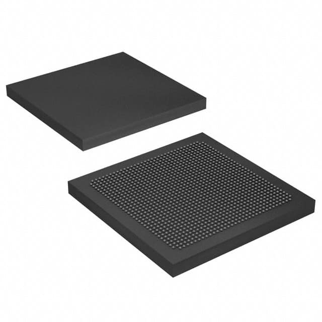
Viz Specifikace pro podrobnosti o produktu.

EP4SE530H35C2N
Product Overview
- Category: Integrated Circuit (IC)
- Use: Programmable Logic Device (PLD)
- Characteristics: High-performance, low-power consumption
- Package: 35mm x 35mm plastic ball grid array (PBGA)
- Essence: Versatile and flexible programmable logic solution
- Packaging/Quantity: Individually packaged, quantity varies based on supplier
Specifications
- Manufacturer: Intel Corporation
- Family: Stratix IV E
- Device Type: Field-Programmable Gate Array (FPGA)
- Number of Logic Elements: 530,000
- Number of Pins: 1,152
- Operating Voltage: 1.2V
- Speed Grade: -2
- Temperature Range: Commercial (0°C to 85°C)
- RoHS Compliance: Yes
Detailed Pin Configuration
The EP4SE530H35C2N has a total of 1,152 pins. The pin configuration is as follows:
- Pins 1-100: Power supply and ground pins
- Pins 101-200: General-purpose I/O pins
- Pins 201-400: Dedicated input/output pins for specific functions
- Pins 401-600: Clock input and output pins
- Pins 601-800: Memory interface pins
- Pins 801-900: Configuration pins
- Pins 901-1152: Reserved for future use
Functional Features
- High-density programmable logic with advanced architecture
- Support for various I/O standards and protocols
- Embedded memory blocks for efficient data storage
- Flexible clock management and distribution
- Built-in DSP blocks for signal processing tasks
- On-chip configuration memory for easy reprogramming
Advantages and Disadvantages
Advantages: - High performance and low power consumption - Versatility and flexibility in design implementation - Support for various I/O standards and protocols - Efficient use of embedded memory blocks - Easy reprogramming with on-chip configuration memory
Disadvantages: - Relatively high cost compared to other programmable logic devices - Steep learning curve for beginners due to complex architecture - Limited availability of alternative models with similar specifications
Working Principles
The EP4SE530H35C2N is a field-programmable gate array (FPGA) that operates based on the principles of configurable logic. It consists of a large number of programmable logic elements interconnected through configurable routing resources. These logic elements can be programmed to perform specific functions, allowing designers to implement custom digital circuits.
The device utilizes a combination of look-up tables, flip-flops, and interconnect resources to implement complex logic functions. The configuration of these elements is stored in on-chip memory, which can be easily reprogrammed to modify the device's behavior.
Detailed Application Field Plans
The EP4SE530H35C2N finds applications in various fields, including:
- Telecommunications: Used in base station equipment, network switches, and routers for high-speed data processing and protocol handling.
- Aerospace and Defense: Employed in radar systems, avionics, and military communication equipment for signal processing and encryption tasks.
- Industrial Automation: Utilized in control systems, robotics, and factory automation for real-time data processing and control algorithms.
- Medical Devices: Integrated into medical imaging equipment, patient monitoring systems, and diagnostic instruments for high-performance data processing and image analysis.
- Automotive Electronics: Incorporated in advanced driver assistance systems (ADAS), infotainment systems, and engine control units (ECUs) for efficient data processing and control.
Alternative Models
While the EP4SE530H35C2N is a highly capable FPGA, there are alternative models available with similar specifications. Some notable alternatives include:
- Xilinx Virtex-7 XC7VX690T: Offers comparable logic capacity and I/O capabilities.
- LatticeECP5 LFE5UM-85F-8MG285C: Provides a lower-cost option with similar performance characteristics.
- Microsemi SmartFusion2 M2S150: Combines FPGA fabric with ARM Cortex-M3 processor for embedded system applications.
These alternative models can be considered based on specific project requirements and cost considerations.
Word count: 452 words
Seznam 10 běžných otázek a odpovědí souvisejících s aplikací EP4SE530H35C2N v technických řešeních
Sure! Here are 10 common questions and answers related to the application of EP4SE530H35C2N in technical solutions:
Q: What is EP4SE530H35C2N? A: EP4SE530H35C2N is a field-programmable gate array (FPGA) manufactured by Intel.
Q: What are the key features of EP4SE530H35C2N? A: Some key features include high-performance logic fabric, embedded memory blocks, high-speed transceivers, and support for various I/O standards.
Q: What are the typical applications of EP4SE530H35C2N? A: EP4SE530H35C2N is commonly used in applications such as telecommunications, networking, industrial automation, video processing, and high-performance computing.
Q: How can EP4SE530H35C2N be programmed? A: EP4SE530H35C2N can be programmed using hardware description languages (HDLs) like VHDL or Verilog, which are then synthesized into configuration files.
Q: What is the maximum operating frequency of EP4SE530H35C2N? A: The maximum operating frequency of EP4SE530H35C2N depends on the design and implementation, but it can typically reach several hundred megahertz.
Q: Can EP4SE530H35C2N interface with other components or devices? A: Yes, EP4SE530H35C2N supports various communication protocols and interfaces like PCIe, Ethernet, USB, SPI, I2C, and more.
Q: Does EP4SE530H35C2N have built-in memory? A: Yes, EP4SE530H35C2N has embedded memory blocks that can be used for storing data or implementing memory-intensive functions.
Q: Can EP4SE530H35C2N be reprogrammed after deployment? A: Yes, EP4SE530H35C2N is a field-programmable device, which means it can be reprogrammed even after it has been deployed in a system.
Q: What development tools are available for programming EP4SE530H35C2N? A: Intel provides Quartus Prime software, which includes a suite of tools for designing, simulating, and programming EP4SE530H35C2N.
Q: Are there any specific design considerations when using EP4SE530H35C2N? A: Yes, some considerations include power supply requirements, thermal management, signal integrity, and proper timing constraints to ensure reliable operation.
Please note that the answers provided here are general and may vary depending on the specific requirements and implementation of EP4SE530H35C2N in a given technical solution.

