

Viz Specifikace pro podrobnosti o produktu.
IXTT16N10D2
Introduction
The IXTT16N10D2 is a power MOSFET belonging to the category of semiconductor devices. This entry provides an overview of its basic information, specifications, pin configuration, functional features, advantages and disadvantages, working principles, application field plans, and alternative models.
Basic Information Overview
- Category: Semiconductor Device
- Use: Power switching applications
- Characteristics: High voltage capability, low on-resistance, fast switching speed
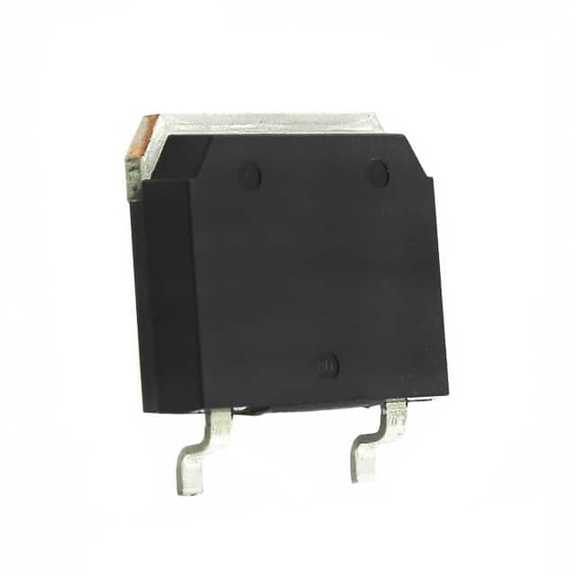
- Package: TO-220AB
- Essence: Power MOSFET for high-performance applications
- Packaging/Quantity: Typically packaged in reels or tubes, quantity varies by manufacturer
Specifications
- Voltage Rating: 100V
- Current Rating: 16A
- On-Resistance: 0.1 Ohm
- Gate Threshold Voltage: 2.5V
- Operating Temperature Range: -55°C to 175°C
Detailed Pin Configuration
The IXTT16N10D2 typically follows the standard pin configuration for a TO-220AB package: 1. Gate (G) 2. Drain (D) 3. Source (S)
Functional Features
- High voltage capability suitable for various power applications
- Low on-resistance leading to reduced power dissipation
- Fast switching speed enabling efficient power control
Advantages and Disadvantages
Advantages
- High voltage capability
- Low on-resistance
- Fast switching speed
Disadvantages
- May require additional circuitry for overvoltage protection
Working Principles
The IXTT16N10D2 operates based on the principles of field-effect transistors, utilizing the control of electric fields to modulate the conductivity of the device. When a sufficient gate-source voltage is applied, the device allows current to flow from drain to source, effectively acting as a switch in power applications.
Detailed Application Field Plans
The IXTT16N10D2 finds extensive use in various power switching applications, including but not limited to: - Switching power supplies - Motor control - Inverters - DC-DC converters - Industrial automation
Detailed and Complete Alternative Models
- IXTT16N10D
- IXTT16N10D1
- IXTT16N10D3
- IXTT16N10D4
In conclusion, the IXTT16N10D2 power MOSFET offers high voltage capability, low on-resistance, and fast switching speed, making it suitable for diverse power switching applications across different industries.
(Word count: 366)
Seznam 10 běžných otázek a odpovědí souvisejících s aplikací IXTT16N10D2 v technických řešeních
What is IXTT16N10D2?
- IXTT16N10D2 is a high voltage, high speed switching NPT trench IGBT designed for various technical solutions requiring efficient power control.
What are the key features of IXTT16N10D2?
- The key features include a high voltage capability, low VCE(sat), fast switching speed, and ruggedness suitable for demanding technical applications.
What technical solutions can IXTT16N10D2 be used in?
- IXTT16N10D2 can be used in applications such as motor drives, induction heating, UPS systems, solar inverters, and welding equipment.
What is the maximum voltage and current rating of IXTT16N10D2?
- IXTT16N10D2 has a maximum voltage rating of 1000V and a continuous collector current rating of 16A.
How does IXTT16N10D2 compare to other similar devices in terms of performance?
- IXTT16N10D2 offers superior performance in terms of switching speed, low saturation voltage, and ruggedness compared to many similar devices.
What are the thermal characteristics of IXTT16N10D2?
- IXTT16N10D2 has excellent thermal performance with low thermal resistance and high junction temperature capability, making it suitable for high-power applications.
Can IXTT16N10D2 be used in parallel configurations for higher current applications?
- Yes, IXTT16N10D2 can be used in parallel configurations to achieve higher current handling capabilities in technical solutions.
Are there any application notes or reference designs available for using IXTT16N10D2?
- Yes, there are application notes and reference designs available from the manufacturer to assist in the proper implementation of IXTT16N10D2 in various technical solutions.
What protection features does IXTT16N10D2 offer for reliable operation in technical solutions?
- IXTT16N10D2 offers built-in protection features such as short-circuit protection, over-temperature protection, and under-voltage lockout to ensure reliable operation in technical solutions.
Where can I find detailed specifications and datasheets for IXTT16N10D2?
- Detailed specifications and datasheets for IXTT16N10D2 can be found on the manufacturer's website or through authorized distributors.