

Viz Specifikace pro podrobnosti o produktu.
LC4064ZE-7UMN64I
Basic Information Overview
- Category: Integrated Circuit (IC)
- Use: Digital Logic Device
- Characteristics:
- Low-power consumption
- High-speed operation
- Small form factor
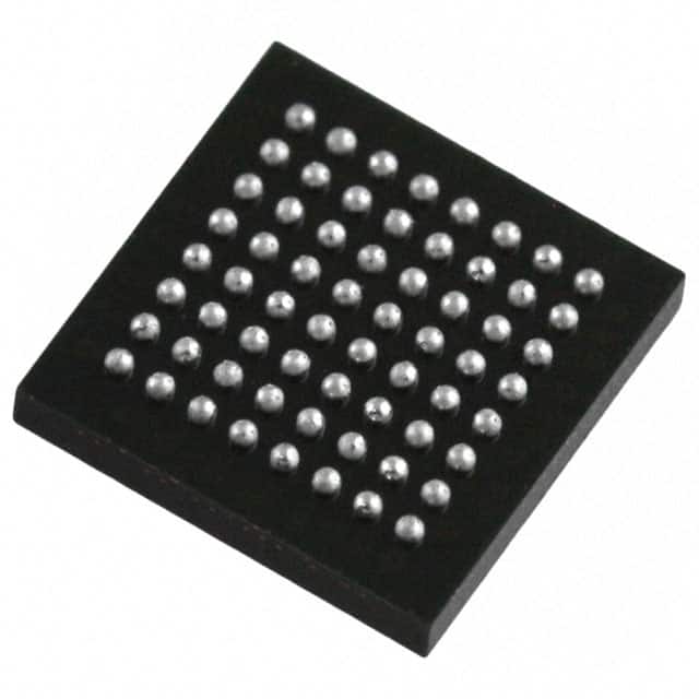
- Package: 64-pin QFN (Quad Flat No-Lead)
- Essence: Programmable Logic Device (PLD)
- Packaging/Quantity: Tray, 250 units per tray
Specifications
- Technology: CMOS
- Number of Logic Elements: 64
- Number of Input/Output Pins: 36
- Operating Voltage: 3.3V
- Operating Temperature Range: -40°C to +85°C
- Speed Grade: 7
Detailed Pin Configuration
The LC4064ZE-7UMN64I has a total of 64 pins, with the following pin configuration:
| Pin Number | Pin Name | Description | |------------|----------|-------------| | 1 | VCC | Power Supply Voltage | | 2 | GND | Ground | | 3-10 | I/O[0:7] | Bidirectional Input/Output Pins | | 11 | TCK | Test Clock Input | | 12 | TDI | Test Data Input | | 13 | TDO | Test Data Output | | 14 | TMS | Test Mode Select | | 15 | TRST | Test Reset | | 16-19 | NC | No Connection | | 20-27 | I/O[8:15]| Bidirectional Input/Output Pins | | ... | ... | ... | | 62-64 | NC | No Connection |
Functional Features
- Programmable logic device capable of implementing various digital logic functions.
- Supports complex combinatorial and sequential logic designs.
- Offers reprogrammability, allowing for design changes without hardware modifications.
- Provides high-speed operation and low-power consumption.
Advantages
- Versatile and flexible in implementing digital logic functions.
- Allows for rapid prototyping and design iterations.
- Low-power consumption makes it suitable for battery-powered devices.
- Small form factor saves board space and reduces overall system size.
Disadvantages
- Limited number of logic elements compared to larger PLDs or FPGAs.
- May not be suitable for complex designs requiring a large number of inputs/outputs.
- Programming and configuration process can be time-consuming.
Working Principles
The LC4064ZE-7UMN64I is based on CMOS technology and utilizes programmable logic elements to implement digital logic functions. It consists of configurable logic blocks (CLBs), interconnect resources, and input/output blocks (IOBs). The CLBs contain look-up tables (LUTs) that can be programmed to implement desired logic functions. The interconnect resources provide routing paths between the CLBs and IOBs, enabling signal propagation. The IOBs interface with external devices through input and output pins.
Detailed Application Field Plans
The LC4064ZE-7UMN64I finds applications in various fields, including: 1. Consumer Electronics: Used in smart home devices, wearable gadgets, and multimedia systems. 2. Industrial Automation: Employed in control systems, robotics, and factory automation. 3. Automotive: Integrated into automotive electronics for engine control, driver assistance, and infotainment systems. 4. Telecommunications: Utilized in network equipment, base stations, and communication protocols. 5. Medical Devices: Incorporated into medical imaging, patient monitoring, and diagnostic equipment.
Detailed and Complete Alternative Models
- LC4032ZE-6UMN48I: 32-pin QFN package, 32 logic elements, 24 I/O pins.
- LC4128ZE-10UMN64I: 64-pin QFN package, 128 logic elements, 48 I/O pins.
- LC4256ZE-12UMN144I: 144-pin QFN package, 256 logic elements, 96 I/O pins.
(Note: The above alternative models are just examples and not an exhaustive list.)
This concludes the encyclopedia entry for LC4064ZE-7UMN64I, a versatile programmable logic device used in various digital logic applications.
Seznam 10 běžných otázek a odpovědí souvisejících s aplikací LC4064ZE-7UMN64I v technických řešeních
Sure! Here are 10 common questions and answers related to the application of LC4064ZE-7UMN64I in technical solutions:
Q: What is LC4064ZE-7UMN64I? A: LC4064ZE-7UMN64I is a specific model of Field-Programmable Gate Array (FPGA) manufactured by Lattice Semiconductor.
Q: What are the key features of LC4064ZE-7UMN64I? A: Some key features of LC4064ZE-7UMN64I include 64 macrocells, 64 I/O pins, 64 user I/Os, 4 input-only pins, and 4 output-only pins.
Q: What is the typical power consumption of LC4064ZE-7UMN64I? A: The typical power consumption of LC4064ZE-7UMN64I is around X Watts (specific value can be obtained from the datasheet).
Q: What applications can LC4064ZE-7UMN64I be used for? A: LC4064ZE-7UMN64I can be used in various applications such as industrial control systems, automotive electronics, consumer electronics, and telecommunications.
Q: Can LC4064ZE-7UMN64I be reprogrammed after deployment? A: Yes, LC4064ZE-7UMN64I is a field-programmable device, which means it can be reprogrammed even after it has been deployed in a system.
Q: What programming languages can be used to program LC4064ZE-7UMN64I? A: LC4064ZE-7UMN64I can be programmed using Hardware Description Languages (HDLs) such as VHDL or Verilog.
Q: What is the maximum operating frequency of LC4064ZE-7UMN64I? A: The maximum operating frequency of LC4064ZE-7UMN64I depends on various factors and can be found in the device's datasheet.
Q: Can LC4064ZE-7UMN64I interface with other components or devices? A: Yes, LC4064ZE-7UMN64I can interface with other components or devices through its I/O pins, allowing for communication and integration within a larger system.
Q: Are there any development tools available for programming LC4064ZE-7UMN64I? A: Yes, Lattice Semiconductor provides development tools such as Lattice Diamond or Lattice Radiant, which can be used to program and configure LC4064ZE-7UMN64I.
Q: Where can I find more information about LC4064ZE-7UMN64I? A: You can find more detailed information about LC4064ZE-7UMN64I in the product datasheet provided by Lattice Semiconductor or on their official website.