Viz Specifikace pro podrobnosti o produktu.

LC4128V-5TN100C
Product Overview
Category: Integrated Circuit (IC)
Use: The LC4128V-5TN100C is a programmable logic device (PLD) that belongs to the family of Complex Programmable Logic Devices (CPLDs). It is designed for digital logic applications and offers high-performance, low-power consumption, and flexibility in circuit design.
Characteristics: - High-density programmable logic device - Low power consumption - Flexible and reconfigurable - Fast propagation delay - Wide operating temperature range
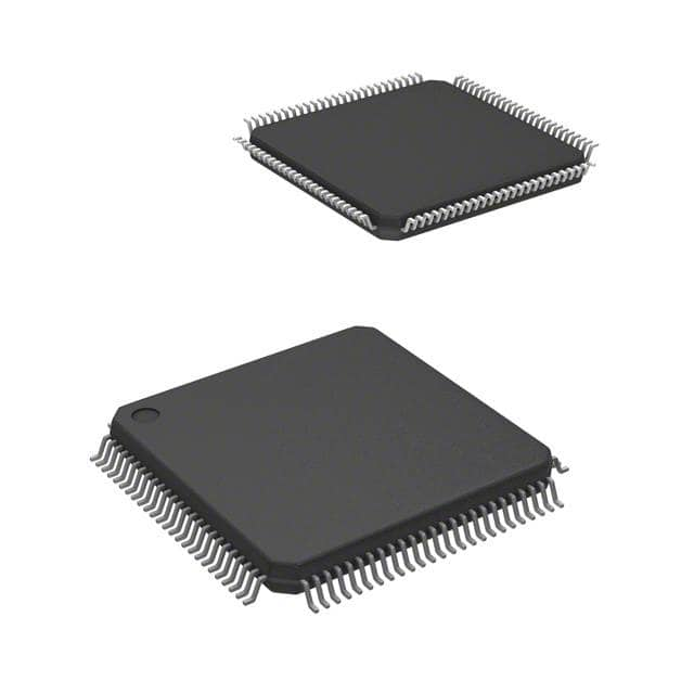
Package: The LC4128V-5TN100C is available in a 100-pin Thin Quad Flat Pack (TQFP) package. This package provides a compact form factor and ease of integration into various electronic systems.
Essence: The essence of the LC4128V-5TN100C lies in its ability to implement complex digital logic functions using programmable interconnects and configurable logic blocks. It allows designers to create custom logic circuits without the need for discrete components.
Packaging/Quantity: The LC4128V-5TN100C is typically sold in reels or trays, with a quantity of 250 units per reel/tray.
Specifications
- Operating Voltage: 3.3V
- Number of Macrocells: 128
- Number of I/O Pins: 96
- Maximum Frequency: 133 MHz
- Programmable Gates: 4,000
- On-Chip Memory: 32 Kbits
- JTAG Boundary Scan Support: Yes
Pin Configuration
The LC4128V-5TN100C has a total of 100 pins, which are assigned different functions based on their configuration. Here is a brief overview of the pinout:
- VCCIO: Power supply pin for I/O buffers.
- GND: Ground reference pin.
- VCCINT: Power supply pin for internal circuitry.
- JTAG: Pins for Joint Test Action Group (JTAG) boundary scan support.
- I/O Pins: Pins for input and output signals.
- Clock Pins: Pins for clock input signals.
- Program Configuration Pins: Pins for programming the device.
For a detailed pin configuration diagram, please refer to the LC4128V-5TN100C datasheet.
Functional Features
The LC4128V-5TN100C offers several functional features that make it suitable for a wide range of digital logic applications:
- Programmability: The device can be programmed to implement various logic functions, allowing designers to create custom circuits.
- Reconfigurability: The PLD can be reprogrammed multiple times, enabling design changes and updates without hardware modifications.
- High-Speed Operation: With a maximum frequency of 133 MHz, the device can handle high-speed digital signals.
- Low Power Consumption: The LC4128V-5TN100C is designed to operate with low power consumption, making it suitable for battery-powered devices.
- JTAG Boundary Scan Support: The device supports JTAG boundary scan, facilitating testing and debugging during the development process.
Advantages and Disadvantages
Advantages: - High-density programmable logic device - Flexible and reconfigurable design - Fast propagation delay for high-speed operation - Low power consumption - JTAG boundary scan support for easy testing and debugging
Disadvantages: - Limited number of macrocells compared to larger CPLDs - Relatively small on-chip memory capacity
Working Principles
The LC4128V-5TN100C operates based on the principles of programmable logic. It consists of configurable logic blocks (CLBs) and programmable interconnects. The CLBs contain look-up tables (LUTs), flip-flops, and other components that can be configured to implement desired logic functions. The programmable interconnects allow for the routing of signals between different CLBs.
During programming, the device is configured using a hardware description language (HDL) or a schematic entry tool. The configuration data is then loaded into the PLD, which configures the internal circuitry accordingly. Once programmed, the device operates based on the defined logic functions.
Application Field Plans
The LC4128V-5TN100C finds applications in various fields where digital logic circuits are required. Some potential application areas include:
- Embedded Systems: The PLD can be used in embedded systems for controlling and interfacing with peripheral devices.
- Communications: It can be utilized in communication systems for protocol handling, signal processing, and data manipulation.
- Industrial Automation: The device can be employed in industrial automation systems for control and monitoring purposes.
- Consumer Electronics: It can be integrated into consumer electronic
Seznam 10 běžných otázek a odpovědí souvisejících s aplikací LC4128V-5TN100C v technických řešeních
Sure! Here are 10 common questions and answers related to the application of LC4128V-5TN100C in technical solutions:
Q: What is LC4128V-5TN100C? A: LC4128V-5TN100C is a specific model of a low-power, high-density programmable logic device (PLD) manufactured by Lattice Semiconductor.
Q: What are the key features of LC4128V-5TN100C? A: The key features of LC4128V-5TN100C include low power consumption, high density, 128 macrocells, 5ns propagation delay, and support for various I/O standards.
Q: What are the typical applications of LC4128V-5TN100C? A: LC4128V-5TN100C is commonly used in applications such as industrial control systems, automotive electronics, telecommunications equipment, and consumer electronics.
Q: How does LC4128V-5TN100C help in reducing power consumption? A: LC4128V-5TN100C incorporates low-power design techniques, such as advanced CMOS technology and power management features, to minimize power consumption during operation.
Q: Can LC4128V-5TN100C be reprogrammed after deployment? A: Yes, LC4128V-5TN100C is a programmable logic device that can be reprogrammed multiple times using appropriate programming tools and software.
Q: What is the maximum number of inputs and outputs supported by LC4128V-5TN100C? A: LC4128V-5TN100C supports up to 128 inputs and outputs, which can be configured as either input or output based on the application requirements.
Q: Does LC4128V-5TN100C support different I/O voltage standards? A: Yes, LC4128V-5TN100C supports various I/O voltage standards, including 3.3V, 2.5V, and 1.8V, making it compatible with a wide range of interface requirements.
Q: Can LC4128V-5TN100C be used in safety-critical applications? A: LC4128V-5TN100C is not specifically designed for safety-critical applications. However, it can be used in such applications if appropriate safety measures are implemented.
Q: What development tools are available for programming LC4128V-5TN100C? A: Lattice Semiconductor provides a range of development tools, including software design tools, programming cables, and evaluation boards, to facilitate the programming and integration of LC4128V-5TN100C.
Q: Are there any specific design considerations when using LC4128V-5TN100C? A: Some design considerations include proper power supply decoupling, signal integrity management, and adherence to timing constraints specified in the device datasheet and application notes.
Please note that these answers are general and may vary depending on specific application requirements and design considerations.

