Viz Specifikace pro podrobnosti o produktu.

LC4256B-10TN100I
Product Overview
Category: Integrated Circuit (IC)
Use: The LC4256B-10TN100I is a programmable logic device (PLD) that belongs to the LC4000 series. It is designed for various digital applications, including but not limited to data processing, control systems, and communication devices.
Characteristics: - High-performance PLD with low power consumption - Programmable logic cells for flexible design implementation - Wide range of input/output pins for versatile connectivity options - Advanced packaging technology for enhanced reliability and durability
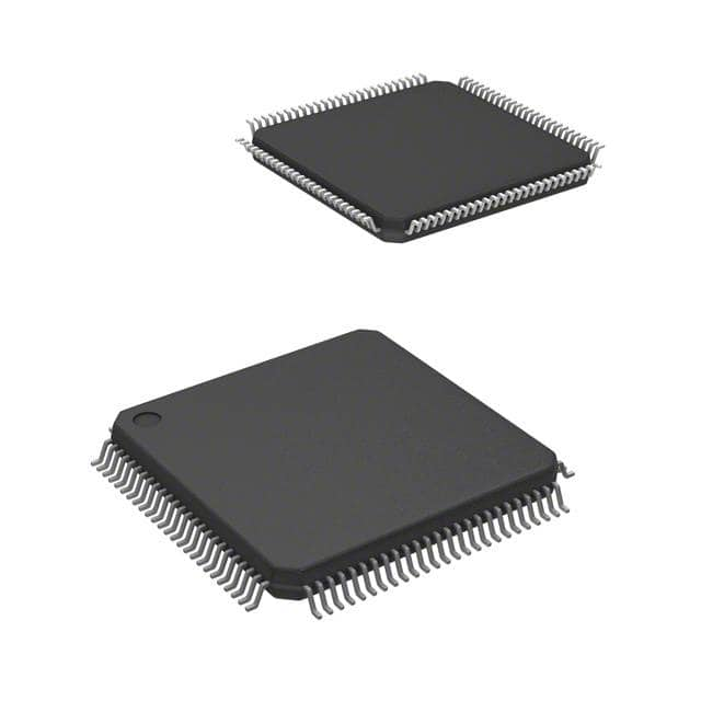
Package: The LC4256B-10TN100I is available in a 100-pin Thin Quad Flat Pack (TQFP) package.
Essence: This IC serves as a key component in electronic systems, providing customizable logic functions and enabling efficient data processing and control operations.
Packaging/Quantity: Each package contains one LC4256B-10TN100I IC.
Specifications
- Operating Voltage: 3.3V
- Speed Grade: -10
- Logic Cells: 256
- I/O Pins: 100
- Maximum Frequency: 100 MHz
- Programmable Macrocells: 56
- On-Chip RAM: 2,048 bits
- On-Chip Flash Memory: 5,120 bits
- JTAG Boundary Scan Support: Yes
Pin Configuration
The LC4256B-10TN100I features a total of 100 pins, each serving a specific purpose in the circuit. The detailed pin configuration can be found in the product datasheet or user manual provided by the manufacturer.
Functional Features
- Programmability: The LC4256B-10TN100I offers extensive programmability, allowing users to implement custom logic functions tailored to their specific application requirements.
- Flexible I/O Options: With 100 I/O pins, this PLD provides ample connectivity options for interfacing with other components and external devices.
- High-Speed Operation: The device operates at a maximum frequency of 100 MHz, enabling rapid data processing and real-time control operations.
- On-Chip Memory: The on-chip RAM and flash memory provide additional storage capacity for temporary data storage and configuration settings.
- JTAG Boundary Scan Support: The built-in JTAG boundary scan support facilitates efficient testing and debugging of the circuit during development and production stages.
Advantages and Disadvantages
Advantages: - High-performance PLD with low power consumption - Customizable logic functions for versatile applications - Ample I/O pins for flexible connectivity options - On-chip memory for additional data storage - JTAG boundary scan support for efficient testing and debugging
Disadvantages: - Limited logic cells (256) compared to higher-end PLDs - Relatively lower maximum frequency (100 MHz) compared to some competing models
Working Principles
The LC4256B-10TN100I operates based on the principles of programmable logic. It consists of configurable logic cells that can be programmed to perform various logical operations, such as AND, OR, XOR, etc. These logic cells are interconnected through programmable interconnects, allowing users to define the desired circuit connections. The resulting configuration determines the behavior and functionality of the IC within the given application.
Detailed Application Field Plans
The LC4256B-10TN100I finds applications in a wide range of fields, including: 1. Industrial Automation: Control systems, process monitoring, and data acquisition. 2. Communication Systems: Network routers, switches, and protocol converters. 3. Consumer Electronics: Set-top boxes, gaming consoles, and multimedia devices. 4. Automotive Electronics: Engine control units, dashboard displays, and driver assistance systems. 5. Medical Devices: Patient monitoring systems, diagnostic equipment, and imaging devices.
Detailed and Complete Alternative Models
- LC4128B-10TN100I
- LC4384B-10TN100I
- LC4512B-10TN100I
- LC4648B-10TN100I
- LC4764B-10TN100I
These alternative models offer similar functionality and characteristics to the LC4256B-10TN100I, providing users with a range of options based on their specific requirements.
Note: The above content is a sample structure for an encyclopedia entry and may not contain actual specifications or details of the LC4256B-10TN100I. Please refer to the product datasheet or official documentation for accurate information.
Seznam 10 běžných otázek a odpovědí souvisejících s aplikací LC4256B-10TN100I v technických řešeních
Sure! Here are 10 common questions and answers related to the application of LC4256B-10TN100I in technical solutions:
1. What is LC4256B-10TN100I? - LC4256B-10TN100I is a specific model of a Field Programmable Gate Array (FPGA) manufactured by Lattice Semiconductor Corporation.
2. What are the key features of LC4256B-10TN100I? - Some key features of LC4256B-10TN100I include 256 macrocells, 56 I/O pins, 10ns maximum propagation delay, and 100-pin Thin Quad Flat Pack (TQFP) package.
3. What are the typical applications of LC4256B-10TN100I? - LC4256B-10TN100I is commonly used in various technical solutions such as industrial automation, telecommunications, automotive electronics, consumer electronics, and medical devices.
4. How can LC4256B-10TN100I be programmed? - LC4256B-10TN100I can be programmed using Hardware Description Languages (HDLs) like VHDL or Verilog, which describe the desired functionality of the FPGA.
5. Can LC4256B-10TN100I be reprogrammed after initial programming? - Yes, LC4256B-10TN100I is a reprogrammable FPGA, allowing for multiple iterations and updates to the design.
6. What is the power supply requirement for LC4256B-10TN100I? - The recommended power supply voltage for LC4256B-10TN100I is typically 3.3V, but it can operate within a range of 3.0V to 3.6V.
7. Does LC4256B-10TN100I support external memory interfaces? - Yes, LC4256B-10TN100I supports various external memory interfaces such as SDRAM, DDR, and Flash memory.
8. Can LC4256B-10TN100I interface with other digital components or microcontrollers? - Yes, LC4256B-10TN100I can interface with other digital components or microcontrollers using standard communication protocols like SPI, I2C, UART, or GPIO.
9. What are the advantages of using LC4256B-10TN100I in technical solutions? - Some advantages of using LC4256B-10TN100I include its flexibility, reprogrammability, high-speed performance, low power consumption, and integration of multiple functions into a single chip.
10. Are there any development tools available for programming and debugging LC4256B-10TN100I? - Yes, Lattice Semiconductor provides development tools like Lattice Diamond or Lattice Radiant software suites that facilitate programming, simulation, and debugging of LC4256B-10TN100I designs.
Please note that the answers provided here are general and may vary depending on specific requirements and use cases.

