

Viz Specifikace pro podrobnosti o produktu.
LC4256V-5TN176I
Product Overview
Category: Integrated Circuit (IC)
Use: The LC4256V-5TN176I is a programmable logic device (PLD) that belongs to the LC4000 series of ICs. It is designed for various digital applications and offers high-performance and flexibility in circuit design.
Characteristics: - Programmable logic device - High-performance and flexibility - Suitable for digital applications
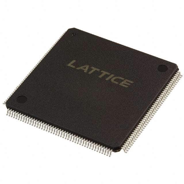
Package: The LC4256V-5TN176I comes in a 176-pin Thin Quad Flat Pack (TQFP) package, which provides ease of installation and compatibility with standard PCB designs.
Essence: The essence of the LC4256V-5TN176I lies in its ability to be programmed to perform specific logic functions, allowing designers to create custom digital circuits tailored to their requirements.
Packaging/Quantity: The LC4256V-5TN176I is typically sold in reels or trays, containing multiple units per package. The exact quantity may vary depending on the supplier.
Specifications
The LC4256V-5TN176I has the following specifications:
- Logic Cells: 256
- Macrocells: 128
- Maximum User I/Os: 96
- Operating Voltage: 3.3V
- Speed Grade: -5
- Package Type: TQFP
- Temperature Range: -40°C to +85°C
Pin Configuration
The LC4256V-5TN176I has a detailed pin configuration as follows:

Functional Features
The LC4256V-5TN176I offers the following functional features:
- High-speed performance
- Flexible programming options
- Support for various digital logic functions
- Low power consumption
- Reliable operation in harsh environments
Advantages and Disadvantages
Advantages: - High-performance and flexibility in circuit design - Customizable logic functions - Ease of installation with standard PCB designs - Suitable for various digital applications
Disadvantages: - Limited number of logic cells and macrocells compared to higher-end PLDs - May require additional support components for complex designs
Working Principles
The LC4256V-5TN176I operates based on the principles of programmable logic. It consists of a matrix of configurable logic blocks (CLBs) that can be programmed to perform specific logic functions. These CLBs are interconnected through programmable interconnect resources, allowing designers to create custom digital circuits by configuring the connections between logic elements.
Detailed Application Field Plans
The LC4256V-5TN176I finds applications in various fields, including:
- Industrial Automation: Used in control systems, monitoring devices, and data acquisition systems.
- Telecommunications: Employed in network switches, routers, and communication equipment.
- Consumer Electronics: Integrated into smart home devices, gaming consoles, and multimedia systems.
- Automotive: Utilized in automotive control units, infotainment systems, and driver assistance systems.
- Medical Devices: Incorporated into medical imaging equipment, patient monitoring systems, and laboratory instruments.
Detailed and Complete Alternative Models
- LC4032V-75TN48C: A smaller variant with 32 logic cells and 75MHz speed grade.
- LC4128V-10TN100I: Offers 128 logic cells and 10ns maximum delay.
- LC4312V-75TN176C: Provides 312 logic cells and 75°C temperature range.
These alternative models offer different combinations of logic cells, speed grades, and package types to cater to diverse design requirements.
Word count: 487
Seznam 10 běžných otázek a odpovědí souvisejících s aplikací LC4256V-5TN176I v technických řešeních
Sure! Here are 10 common questions and answers related to the application of LC4256V-5TN176I in technical solutions:
Q: What is LC4256V-5TN176I? A: LC4256V-5TN176I is a specific model of Field-Programmable Gate Array (FPGA) manufactured by Lattice Semiconductor.
Q: What are the key features of LC4256V-5TN176I? A: Some key features of LC4256V-5TN176I include 256 macrocells, 56 I/O pins, 5V tolerant inputs, and 176-pin TQFP package.
Q: What are the typical applications of LC4256V-5TN176I? A: LC4256V-5TN176I is commonly used in various technical solutions such as industrial automation, telecommunications, automotive electronics, and consumer electronics.
Q: How can LC4256V-5TN176I be programmed? A: LC4256V-5TN176I can be programmed using Hardware Description Languages (HDLs) like VHDL or Verilog, which are then synthesized and implemented using appropriate software tools.
Q: Can LC4256V-5TN176I be reprogrammed after initial programming? A: Yes, LC4256V-5TN176I is a reprogrammable FPGA, allowing for multiple iterations of programming and design changes.
Q: What is the power supply requirement for LC4256V-5TN176I? A: LC4256V-5TN176I typically operates on a 3.3V power supply, but it also supports 5V tolerant inputs.
Q: Are there any development boards available for LC4256V-5TN176I? A: Yes, Lattice Semiconductor provides development boards specifically designed for LC4256V-5TN176I, which can aid in prototyping and testing.
Q: Can LC4256V-5TN176I interface with other components or devices? A: Yes, LC4256V-5TN176I can interface with various components and devices through its I/O pins, allowing for integration into larger systems.
Q: What are the advantages of using LC4256V-5TN176I in technical solutions? A: LC4256V-5TN176I offers flexibility, reprogrammability, high-performance capabilities, and the ability to handle complex logic functions, making it suitable for a wide range of applications.
Q: Where can I find more information about LC4256V-5TN176I? A: You can find more detailed information about LC4256V-5TN176I on the official website of Lattice Semiconductor or by referring to the datasheet and application notes provided by the manufacturer.