

Viz Specifikace pro podrobnosti o produktu.
LC4256V-75FT256BI
Product Overview
Category
The LC4256V-75FT256BI belongs to the category of Field-Programmable Gate Arrays (FPGAs).
Use
This product is primarily used in digital logic circuits for various applications such as telecommunications, automotive, industrial control systems, and consumer electronics.
Characteristics
- High-performance FPGA with advanced features
- Flexible and reconfigurable design
- Low power consumption
- Large number of programmable logic elements
- High-speed interfaces for efficient data transfer
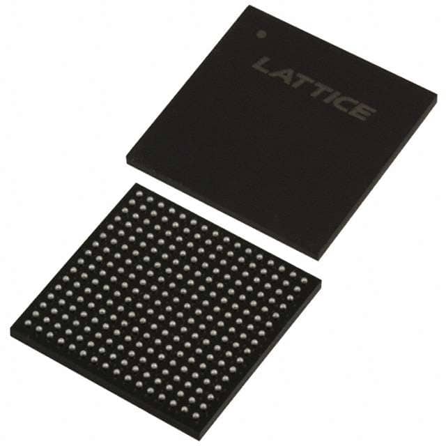
Package
The LC4256V-75FT256BI comes in a compact package that ensures easy integration into electronic systems. It is designed to be mounted on printed circuit boards (PCBs) using surface mount technology (SMT).
Essence
The essence of the LC4256V-75FT256BI lies in its ability to provide a customizable digital logic solution, allowing designers to implement complex functionality without the need for custom hardware.
Packaging/Quantity
The LC4256V-75FT256BI is typically packaged in reels or trays, depending on the manufacturer's specifications. The quantity per package may vary, but it is commonly available in quantities of 100 or more.
Specifications
- Logic Cells: 4256
- Maximum Operating Frequency: 75 MHz
- Programmable I/O Pins: 256
- Embedded Memory: 256 Kbits
- Operating Voltage: 3.3V
- Package Type: Fine-pitch Ball Grid Array (FBGA)
- Temperature Range: -40°C to +85°C
Detailed Pin Configuration
The LC4256V-75FT256BI has a well-defined pin configuration that enables easy connectivity and integration within a system. The detailed pinout can be found in the product datasheet provided by the manufacturer.
Functional Features
- Configurable logic blocks for implementing custom digital circuits
- Programmable interconnects for flexible routing of signals
- Dedicated high-speed input/output (I/O) interfaces
- On-chip memory elements for data storage
- Clock management resources for precise timing control
Advantages and Disadvantages
Advantages
- Versatile and adaptable to various applications
- Reduced development time and cost compared to custom hardware solutions
- Reconfigurable design allows for iterative development and upgrades
- High-performance capabilities for demanding tasks
- Low power consumption for energy-efficient designs
Disadvantages
- Steeper learning curve compared to traditional fixed-function integrated circuits
- Limited resources may restrict the complexity of designs
- Higher cost per unit compared to mass-produced standard components
Working Principles
The LC4256V-75FT256BI operates based on the principles of field-programmable gate arrays. It consists of configurable logic blocks interconnected through programmable routing resources. The device can be programmed using hardware description languages or graphical tools, allowing designers to define the desired functionality.
Detailed Application Field Plans
The LC4256V-75FT256BI finds application in a wide range of fields, including: 1. Telecommunications: Used in network equipment, base stations, and communication protocols. 2. Automotive: Employed in automotive electronics for engine control, driver assistance systems, and infotainment. 3. Industrial Control Systems: Utilized in automation, robotics, and process control systems. 4. Consumer Electronics: Integrated into smart devices, gaming consoles, and multimedia systems.
Detailed and Complete Alternative Models
- LC4128V-75TN100C: A smaller variant with 4128 logic cells and 100-pin Thin Quad Flat Pack (TQFP) package.
- LC4384V-120FTN256C: A higher-capacity FPGA with 4384 logic cells, 120 MHz operating frequency, and 256-pin TQFP package.
- LC4512V-75TN176I: An intermediate model with 4512 logic cells, 75 MHz operating frequency, and 176-pin Thin Quad Flat Pack No-Lead (TQFN) package.
These alternative models provide different options based on the specific requirements of the application.
In conclusion, the LC4256V-75FT256BI is a versatile FPGA that offers high-performance capabilities, flexibility, and reconfigurability. It finds applications in various fields and provides designers with a customizable digital logic solution. Despite some limitations, its advantages outweigh the disadvantages, making it a valuable component for modern electronic systems.
Seznam 10 běžných otázek a odpovědí souvisejících s aplikací LC4256V-75FT256BI v technických řešeních
Sure! Here are 10 common questions and answers related to the application of LC4256V-75FT256BI in technical solutions:
1. What is LC4256V-75FT256BI? - LC4256V-75FT256BI is a specific model of Field Programmable Gate Array (FPGA) manufactured by Lattice Semiconductor.
2. What are the key features of LC4256V-75FT256BI? - The key features of LC4256V-75FT256BI include 256 macrocells, 75MHz maximum operating frequency, 5V tolerant I/O pins, and 256-pin FineLine BGA package.
3. What are the typical applications of LC4256V-75FT256BI? - LC4256V-75FT256BI is commonly used in various technical solutions such as industrial automation, telecommunications, automotive electronics, medical devices, and consumer electronics.
4. How can LC4256V-75FT256BI be programmed? - LC4256V-75FT256BI can be programmed using Hardware Description Languages (HDLs) like VHDL or Verilog, which describe the desired functionality of the FPGA.
5. Can LC4256V-75FT256BI be reprogrammed after initial programming? - Yes, LC4256V-75FT256BI is a reprogrammable FPGA, allowing for multiple iterations and updates to the design.
6. What tools are required to program LC4256V-75FT256BI? - To program LC4256V-75FT256BI, you will need a compatible development board, a programming cable, and the appropriate software provided by Lattice Semiconductor.
7. Is there any documentation available for LC4256V-75FT256BI? - Yes, Lattice Semiconductor provides detailed documentation including datasheets, user guides, and application notes for LC4256V-75FT256BI on their official website.
8. Can LC4256V-75FT256BI interface with other components or devices? - Yes, LC4256V-75FT256BI can interface with various components and devices through its I/O pins, supporting protocols like SPI, I2C, UART, and more.
9. What is the power supply requirement for LC4256V-75FT256BI? - LC4256V-75FT256BI requires a 3.3V power supply for normal operation.
10. Are there any known limitations or considerations when using LC4256V-75FT256BI? - Some considerations include the limited number of macrocells, the maximum operating frequency, and the need for proper heat dissipation in high-performance applications. Additionally, it's important to carefully review the datasheet and user guide for specific details and guidelines related to the device's usage.
Please note that these answers are general and may vary depending on the specific requirements and use cases. It's always recommended to refer to the official documentation and consult with technical experts for accurate information.