

Viz Specifikace pro podrobnosti o produktu.
LC5256MV-5FN256I
Product Overview
Category: Integrated Circuit (IC)
Use: The LC5256MV-5FN256I is a programmable logic device (PLD) that belongs to the family of Complex Programmable Logic Devices (CPLDs). It is designed for use in various electronic applications where digital logic functions need to be implemented.
Characteristics: - High-density programmable logic device - Low power consumption - Fast performance - Flexible and reprogrammable - Wide range of input/output pins - Small form factor
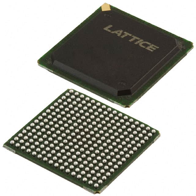
Package: The LC5256MV-5FN256I is available in a 256-pin Fine-Pitch Ball Grid Array (FBGA) package. This package offers excellent thermal and electrical performance, ensuring reliable operation even in demanding environments.
Essence: The essence of the LC5256MV-5FN256I lies in its ability to provide a highly integrated solution for implementing complex digital logic functions. It offers designers the flexibility to create custom logic circuits tailored to their specific application requirements.
Packaging/Quantity: The LC5256MV-5FN256I is typically sold individually in anti-static packaging to prevent damage during transportation and handling.
Specifications
- Number of Logic Elements: 2560
- Maximum User I/O Pins: 192
- Operating Voltage: 3.3V
- Operating Temperature Range: -40°C to 85°C
- Speed Grade: 5 (Fastest)
- JTAG Boundary Scan Support: Yes
Pin Configuration
The LC5256MV-5FN256I has a total of 256 pins, each serving a specific purpose in the circuit design. The detailed pin configuration can be found in the product datasheet provided by the manufacturer.
Functional Features
- High-speed internal architecture for efficient logic implementation
- Programmable interconnect resources for flexible routing of signals
- On-chip memory elements for storage and retrieval of data
- Clock management circuitry for synchronization of operations
- Built-in JTAG boundary scan support for easy testing and debugging
Advantages and Disadvantages
Advantages: - High-density integration allows for complex logic functions in a small footprint - Reprogrammability enables design changes without hardware modifications - Low power consumption makes it suitable for portable and battery-powered devices - Fast performance ensures efficient execution of digital logic operations - Wide range of I/O pins provides flexibility in interfacing with other components
Disadvantages: - Limited number of logic elements compared to larger FPGA devices - Relatively higher cost per unit compared to simpler programmable logic devices - Steeper learning curve for designers unfamiliar with CPLD programming
Working Principles
The LC5256MV-5FN256I operates based on the principles of programmable logic. It consists of an array of configurable logic blocks (CLBs) interconnected through programmable routing resources. The CLBs can be programmed to implement various logic functions, such as AND, OR, XOR, and more. The interconnect resources allow designers to route signals between different CLBs, enabling the creation of complex digital circuits.
Application Field Plans
The LC5256MV-5FN256I finds applications in a wide range of fields, including but not limited to: - Industrial automation - Communication systems - Consumer electronics - Automotive electronics - Medical devices - Aerospace and defense
Its versatility and programmability make it suitable for diverse applications that require custom logic implementation.
Alternative Models
For those seeking alternative options, several other CPLDs are available in the market. Some notable alternatives to the LC5256MV-5FN256I include: - Altera MAX V CPLD series - Xilinx CoolRunner-II CPLD series - Lattice MachXO2 CPLD series
These alternative models offer similar functionality and can be considered based on specific project requirements.
In conclusion, the LC5256MV-5FN256I is a high-density programmable logic device that provides designers with the flexibility to implement complex digital logic functions. Its small form factor, low power consumption, and fast performance make it suitable for various electronic applications. While it has certain limitations, its advantages outweigh the disadvantages, making it a popular choice in the field of programmable logic.
Seznam 10 běžných otázek a odpovědí souvisejících s aplikací LC5256MV-5FN256I v technických řešeních
Sure! Here are 10 common questions and answers related to the application of LC5256MV-5FN256I in technical solutions:
Q: What is LC5256MV-5FN256I? A: LC5256MV-5FN256I is a specific model of Field Programmable Gate Array (FPGA) manufactured by Lattice Semiconductor.
Q: What are the key features of LC5256MV-5FN256I? A: Some key features of LC5256MV-5FN256I include 256-pin Fine-Pitch Ball Grid Array (FBGA) package, 5V operation, and 256 macrocells.
Q: What are the typical applications of LC5256MV-5FN256I? A: LC5256MV-5FN256I is commonly used in various technical solutions such as industrial automation, motor control, communication systems, and automotive electronics.
Q: How can I program LC5256MV-5FN256I? A: LC5256MV-5FN256I can be programmed using hardware description languages (HDL) like VHDL or Verilog, which are then synthesized and implemented using appropriate software tools provided by Lattice Semiconductor.
Q: Can LC5256MV-5FN256I be reprogrammed after initial programming? A: Yes, LC5256MV-5FN256I is a reprogrammable FPGA, allowing for multiple programming cycles during its lifetime.
Q: What is the power supply requirement for LC5256MV-5FN256I? A: LC5256MV-5FN256I operates at a voltage of 5V, so it requires a stable 5V power supply.
Q: Does LC5256MV-5FN256I support external memory interfaces? A: Yes, LC5256MV-5FN256I supports various external memory interfaces like SRAM, SDRAM, and Flash memory.
Q: Can LC5256MV-5FN256I interface with other digital components or microcontrollers? A: Yes, LC5256MV-5FN256I can interface with other digital components or microcontrollers through standard communication protocols like SPI, I2C, UART, or GPIO pins.
Q: What is the maximum operating frequency of LC5256MV-5FN256I? A: The maximum operating frequency of LC5256MV-5FN256I depends on the design and implementation, but it can typically reach frequencies in the range of tens to hundreds of megahertz (MHz).
Q: Are there any development boards or evaluation kits available for LC5256MV-5FN256I? A: Yes, Lattice Semiconductor provides development boards and evaluation kits specifically designed for LC5256MV-5FN256I, which include necessary hardware and software tools for prototyping and testing applications.
Please note that the specific details and answers may vary depending on the manufacturer's documentation and specifications for LC5256MV-5FN256I.