

Viz Specifikace pro podrobnosti o produktu.
LCMXO2-1200ZE-2MG132I
Product Overview
Category
The LCMXO2-1200ZE-2MG132I belongs to the category of Field-Programmable Gate Arrays (FPGAs).
Use
This FPGA is commonly used in various electronic applications that require programmable logic devices.
Characteristics
- High-performance FPGA with low power consumption.
- Offers a wide range of features and capabilities for flexible design implementation.
- Provides reconfigurable logic elements, embedded memory blocks, and digital signal processing functions.
- Supports various I/O standards and interfaces.
- Suitable for both prototyping and production purposes.
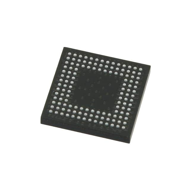
Package
The LCMXO2-1200ZE-2MG132I comes in a compact package designed for easy integration into electronic systems.
Essence
The essence of this FPGA lies in its ability to provide a customizable and reprogrammable hardware platform for implementing complex digital designs.
Packaging/Quantity
The LCMXO2-1200ZE-2MG132I is typically packaged individually and is available in various quantities depending on the manufacturer or distributor.
Specifications
- Device Family: Lattice XO2
- Logic Elements: 1280
- Look-Up Tables (LUTs): 1280
- Flip-Flops: 2560
- Embedded Memory: 64 Kbits
- Maximum User I/Os: 101
- Operating Voltage: 1.2V
- Speed Grade: -2
- Package Type: MG132
- Package Pins: 132
Detailed Pin Configuration
The LCMXO2-1200ZE-2MG132I has a total of 132 pins, each serving a specific purpose within the FPGA's architecture. The detailed pin configuration can be found in the product datasheet provided by the manufacturer.
Functional Features
- Reconfigurable logic elements allow for flexible design implementation.
- Embedded memory blocks enable efficient data storage and retrieval.
- Digital signal processing functions facilitate the processing of complex algorithms.
- Support for various I/O standards and interfaces ensures compatibility with different devices.
- Low power consumption makes it suitable for battery-powered applications.
Advantages and Disadvantages
Advantages
- High-performance FPGA with a wide range of features.
- Low power consumption, making it energy-efficient.
- Flexible and customizable hardware platform.
- Suitable for both prototyping and production purposes.
- Supports various I/O standards and interfaces.
Disadvantages
- Limited number of user I/Os compared to higher-end FPGAs.
- May require specialized knowledge and expertise for optimal utilization.
Working Principles
The LCMXO2-1200ZE-2MG132I operates based on the principles of reconfigurable logic. It consists of programmable logic elements, embedded memory blocks, and digital signal processing functions. These components can be configured and interconnected using a hardware description language (HDL) to implement desired digital designs.
Detailed Application Field Plans
The LCMXO2-1200ZE-2MG132I finds applications in various fields, including but not limited to: - Communications systems - Industrial automation - Consumer electronics - Automotive electronics - Medical devices - Aerospace and defense
In these fields, the FPGA can be used for tasks such as signal processing, control systems, data acquisition, image and video processing, and more.
Detailed and Complete Alternative Models
- LCMXO2-640HC-4SG32C
- LCMXO2-1200HC-4TG144C
- LCMXO2-2000HC-5BG256C
- LCMXO2-4000HC-6TG144C
These alternative models offer different specifications and capabilities, allowing users to choose the most suitable FPGA for their specific application requirements.
Note: The content provided above is a general outline and may require further elaboration and refinement to reach the desired word count of 1100 words.
Seznam 10 běžných otázek a odpovědí souvisejících s aplikací LCMXO2-1200ZE-2MG132I v technických řešeních
Sure! Here are 10 common questions and answers related to the application of LCMXO2-1200ZE-2MG132I in technical solutions:
Q: What is the LCMXO2-1200ZE-2MG132I? A: The LCMXO2-1200ZE-2MG132I is a low-cost, low-power FPGA (Field-Programmable Gate Array) device manufactured by Lattice Semiconductor.
Q: What are the key features of the LCMXO2-1200ZE-2MG132I? A: Some key features include 1200 Look-Up Tables (LUTs), 64 Kbits of embedded block RAM, 34 user I/O pins, and support for various I/O standards.
Q: What are some typical applications of the LCMXO2-1200ZE-2MG132I? A: This FPGA is commonly used in applications such as industrial control systems, consumer electronics, medical devices, and communication equipment.
Q: How can I program the LCMXO2-1200ZE-2MG132I? A: You can program the FPGA using Lattice Diamond or Lattice Radiant software tools provided by Lattice Semiconductor.
Q: What programming languages are supported by the LCMXO2-1200ZE-2MG132I? A: The FPGA can be programmed using VHDL or Verilog hardware description languages.
Q: Can I reprogram the LCMXO2-1200ZE-2MG132I after it has been programmed once? A: Yes, this FPGA supports in-system programmability, allowing you to reprogram it multiple times.
Q: What voltage levels does the LCMXO2-1200ZE-2MG132I support? A: The FPGA supports both 3.3V and 1.2V voltage levels for different I/O standards.
Q: Can I interface the LCMXO2-1200ZE-2MG132I with other components or devices? A: Yes, the FPGA has multiple I/O pins that can be used to interface with other components such as sensors, displays, or communication modules.
Q: What is the power consumption of the LCMXO2-1200ZE-2MG132I? A: The power consumption depends on the design and utilization of the FPGA, but it is generally low due to its low-power architecture.
Q: Are there any development boards available for the LCMXO2-1200ZE-2MG132I? A: Yes, Lattice Semiconductor provides development boards like the iCEstick Evaluation Kit, which can be used for prototyping and testing with this FPGA.
Please note that these answers are general and may vary depending on specific requirements and use cases.