

Viz Specifikace pro podrobnosti o produktu.
LCMXO2-256HC-5UMG64I
Product Overview
Category
The LCMXO2-256HC-5UMG64I belongs to the category of Field Programmable Gate Arrays (FPGAs).
Use
FPGAs are integrated circuits that can be programmed and reprogrammed to perform various digital functions. The LCMXO2-256HC-5UMG64I is specifically designed for applications requiring low power consumption and high performance.
Characteristics
- Low power consumption
- High performance
- Small form factor
- Flexible and reprogrammable
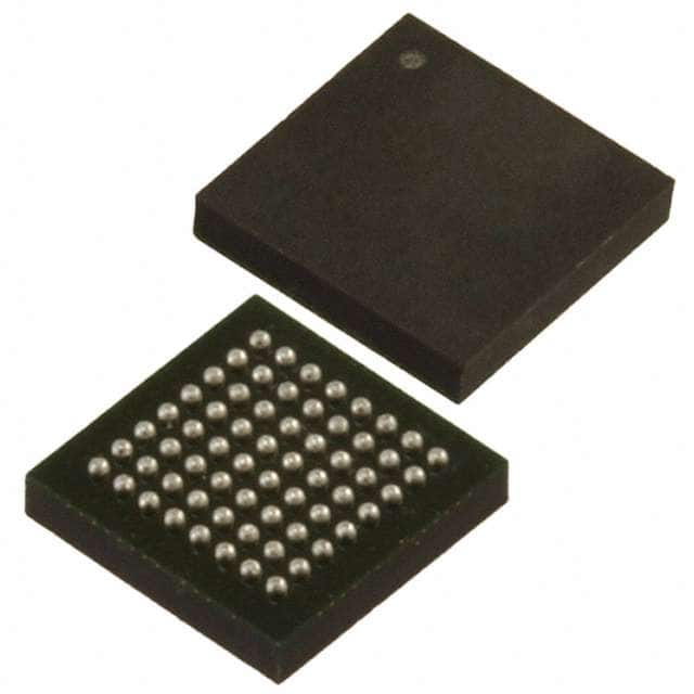
Package
The LCMXO2-256HC-5UMG64I comes in a compact 64-pin Micro Fine Ball Grid Array (BGA) package.
Essence
The essence of the LCMXO2-256HC-5UMG64I lies in its ability to provide a customizable digital logic solution with low power consumption and high performance.
Packaging/Quantity
The LCMXO2-256HC-5UMG64I is typically sold in reels or trays, with each reel or tray containing a specific quantity of units. The exact packaging and quantity may vary depending on the supplier.
Specifications
- FPGA Family: Lattice XO2
- Logic Elements: 256
- User I/Os: 48
- Block RAM: 4 Kbits
- Operating Voltage: 1.2V
- Speed Grade: -5
- Package Type: Micro Fine BGA
- Package Pins: 64
- Temperature Range: Commercial (0°C to 85°C)
- RoHS Compliant: Yes
Detailed Pin Configuration
The LCMXO2-256HC-5UMG64I has a total of 64 pins. The pin configuration is as follows:
- Pin 1: VCCIO
- Pin 2: GND
- Pin 3: IO_0
- Pin 4: IO_1
- ...
- Pin 63: IO_62
- Pin 64: IO_63
Please refer to the datasheet for a complete pin configuration diagram.
Functional Features
The LCMXO2-256HC-5UMG64I offers several functional features, including:
- Programmable logic elements
- Dedicated input/output pins
- Block RAM for data storage
- Clock management resources
- Built-in security features
- JTAG programming interface
Advantages and Disadvantages
Advantages
- Low power consumption enables energy-efficient designs
- High performance allows for complex digital processing tasks
- Small form factor saves board space
- Reprogrammability provides flexibility for design changes
Disadvantages
- Limited number of logic elements compared to larger FPGAs
- Less I/O pins available compared to higher-end models
- May require additional external components for certain applications
Working Principles
The LCMXO2-256HC-5UMG64I operates based on the principles of configurable logic. It consists of programmable logic elements that can be interconnected to create custom digital circuits. The device is programmed using Hardware Description Languages (HDL) such as VHDL or Verilog, which define the desired functionality of the circuit. Once programmed, the FPGA executes the specified logic operations.
Detailed Application Field Plans
The LCMXO2-256HC-5UMG64I finds applications in various fields, including:
- Embedded Systems: Used for implementing custom digital interfaces and control systems in embedded devices.
- Communications: Employed in networking equipment for protocol handling and data processing.
- Industrial Automation: Utilized for controlling and monitoring industrial processes and machinery.
- Consumer Electronics: Integrated into devices like gaming consoles and multimedia systems for enhanced functionality.
- Automotive: Used in automotive electronics for functions such as engine control, driver assistance, and infotainment systems.
Detailed and Complete Alternative Models
- LCMXO2-1200HC-4TG100C
- LCMXO2-2000HC-6TG144C
- LCMXO2-4000HC-6TG144C
- LCMXO2-7000HC-7BG256C
These alternative models offer higher logic capacity and more I/O pins, catering to different design requirements.
Note: The content provided above is a sample entry and may not reflect the actual specifications or details of the LCMXO2-256HC-5UMG64I FPGA.
Seznam 10 běžných otázek a odpovědí souvisejících s aplikací LCMXO2-256HC-5UMG64I v technických řešeních
What is the maximum operating frequency of LCMXO2-256HC-5UMG64I?
- The maximum operating frequency of LCMXO2-256HC-5UMG64I is 100 MHz.What are the typical applications for LCMXO2-256HC-5UMG64I?
- LCMXO2-256HC-5UMG64I is commonly used in consumer electronics, industrial automation, and communication systems.Can LCMXO2-256HC-5UMG64I be used in battery-powered devices?
- Yes, LCMXO2-256HC-5UMG64I has low power consumption and can be used in battery-powered devices.What are the available I/O standards for LCMXO2-256HC-5UMG64I?
- LCMXO2-256HC-5UMG64I supports various I/O standards including LVCMOS, LVTTL, and SSTL.Is LCMXO2-256HC-5UMG64I suitable for high-reliability applications?
- Yes, LCMXO2-256HC-5UMG64I is suitable for high-reliability applications due to its robust design and performance.What development tools are available for programming LCMXO2-256HC-5UMG64I?
- Development tools such as Lattice Diamond Programmer and iCEcube2 are available for programming LCMXO2-256HC-5UMG64I.Can LCMXO2-256HC-5UMG64I be used in automotive applications?
- Yes, LCMXO2-256HC-5UMG64I is qualified for automotive applications and meets industry standards.What are the temperature range specifications for LCMXO2-256HC-5UMG64I?
- LCMXO2-256HC-5UMG64I operates within a temperature range of -40°C to 125°C.Does LCMXO2-256HC-5UMG64I support secure configuration features?
- Yes, LCMXO2-256HC-5UMG64I supports secure configuration features for enhanced system security.Are there any known compatibility issues with using LCMXO2-256HC-5UMG64I with other components?
- LCMXO2-256HC-5UMG64I is designed to be compatible with a wide range of components, and there are no known compatibility issues.