

Viz Specifikace pro podrobnosti o produktu.
LCMXO2-256HC-6SG48I
Product Overview
Category: Programmable Logic Device (PLD)
Use: The LCMXO2-256HC-6SG48I is a high-capacity PLD designed for various digital logic applications. It offers flexibility and customization options, making it suitable for a wide range of projects.
Characteristics: - High capacity: The LCMXO2-256HC-6SG48I has a large number of logic elements, allowing for complex designs. - Low power consumption: It operates at low power levels, making it energy-efficient. - Small form factor: The device comes in a compact package, saving space on the circuit board. - Fast performance: It offers high-speed operation, enabling quick data processing.
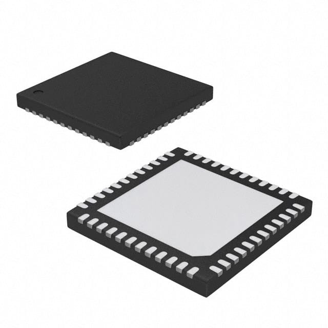
Package: The LCMXO2-256HC-6SG48I is available in a 48-pin small-grid array (SGA) package.
Essence: The essence of the LCMXO2-256HC-6SG48I lies in its ability to provide programmable logic capabilities, allowing designers to implement custom digital circuits.
Packaging/Quantity: The LCMXO2-256HC-6SG48I is typically sold individually or in small quantities, depending on the supplier.
Specifications
- Logic Elements: 256
- Look-Up Tables (LUTs): 1280
- Flip-Flops: 640
- Maximum Frequency: 100 MHz
- Operating Voltage: 1.2V
- I/O Pins: 36
- Configuration Memory: Flash-based
Detailed Pin Configuration
The LCMXO2-256HC-6SG48I has a total of 48 pins, each serving a specific purpose. Here is a brief overview of some key pin functions:
- VCCIO: Power supply pin for I/O buffers.
- GND: Ground reference pin.
- JTAGTMS, JTAGTCK, JTAGTDI, JTAGTDO: Pins used for Joint Test Action Group (JTAG) boundary scan testing and programming.
- IO[0:35]: General-purpose I/O pins for connecting to external devices.
For a complete pin configuration diagram, please refer to the manufacturer's datasheet.
Functional Features
The LCMXO2-256HC-6SG48I offers several functional features that enhance its usability:
- Programmable Logic: The device allows users to implement custom logic functions using Look-Up Tables (LUTs) and flip-flops.
- I/O Flexibility: It provides a sufficient number of I/O pins for interfacing with external devices.
- Flash-based Configuration: The PLD can be reprogrammed multiple times using flash memory technology.
- Low Power Operation: The LCMXO2-256HC-6SG48I is designed to operate at low power levels, reducing energy consumption.
Advantages and Disadvantages
Advantages: - High capacity and performance for complex designs. - Low power consumption. - Small form factor. - Flexible and customizable.
Disadvantages: - Limited I/O pins compared to larger PLDs. - Higher cost compared to simpler logic devices.
Working Principles
The LCMXO2-256HC-6SG48I operates based on the principles of programmable logic. It consists of configurable logic blocks (CLBs), interconnect resources, and I/O elements. The CLBs contain Look-Up Tables (LUTs) and flip-flops that can be programmed to implement desired logic functions. The interconnect resources allow for routing signals between different CLBs and I/O pins. By configuring the CLBs and interconnect resources, designers can create custom digital circuits.
Detailed Application Field Plans
The LCMXO2-256HC-6SG48I finds applications in various fields, including:
- Embedded Systems: It can be used to implement control and communication functions in embedded systems.
- Digital Signal Processing: The PLD can be utilized for implementing signal processing algorithms in real-time applications.
- Industrial Automation: It enables the design of custom logic circuits for automation and control systems.
- Communications: The device can be employed in networking equipment for protocol handling and data manipulation.
- Consumer Electronics: It finds use in consumer electronic devices for custom functionality implementation.
Detailed and Complete Alternative Models
- Xilinx Spartan-6 XC6SLX9: A similar PLD with lower capacity but cost-effective.
- Altera Cyclone IV EP4CE6: Another option with comparable capacity and performance.
- Microchip ATF150x: A flash-based PLD offering similar features.
These alternative models provide options based on specific project requirements, budget constraints, and availability.
*Note: The content provided above is a sample structure for
Seznam 10 běžných otázek a odpovědí souvisejících s aplikací LCMXO2-256HC-6SG48I v technických řešeních
Sure! Here are 10 common questions and answers related to the application of LCMXO2-256HC-6SG48I in technical solutions:
Q: What is the LCMXO2-256HC-6SG48I? A: The LCMXO2-256HC-6SG48I is a low-cost, low-power FPGA (Field-Programmable Gate Array) device manufactured by Lattice Semiconductor.
Q: What are the key features of LCMXO2-256HC-6SG48I? A: The key features include 256 LUTs (Look-Up Tables), 6400 flip-flops, 64 I/O pins, 4 PLLs (Phase-Locked Loops), and support for various interfaces like SPI, I2C, UART, etc.
Q: What are some typical applications of LCMXO2-256HC-6SG48I? A: LCMXO2-256HC-6SG48I is commonly used in applications such as industrial control systems, consumer electronics, medical devices, communication equipment, and IoT (Internet of Things) devices.
Q: How can I program the LCMXO2-256HC-6SG48I? A: The LCMXO2-256HC-6SG48I can be programmed using Lattice Diamond or Lattice Radiant software tools, which provide a graphical interface for designing and programming the FPGA.
Q: What voltage levels does LCMXO2-256HC-6SG48I support? A: The LCMXO2-256HC-6SG48I supports both 3.3V and 1.2V voltage levels, making it compatible with a wide range of digital systems.
Q: Can I use LCMXO2-256HC-6SG48I for high-speed applications? A: While LCMXO2-256HC-6SG48I is not specifically designed for high-speed applications, it can still handle moderate-speed designs with proper optimization techniques.
Q: Does LCMXO2-256HC-6SG48I support external memory interfaces? A: Yes, LCMXO2-256HC-6SG48I supports various external memory interfaces like SPI Flash, SDRAM, and SRAM, allowing for larger storage and data processing capabilities.
Q: Can I use LCMXO2-256HC-6SG48I in battery-powered devices? A: Yes, LCMXO2-256HC-6SG48I is known for its low-power consumption, making it suitable for battery-powered devices where power efficiency is crucial.
Q: Are there any development boards available for LCMXO2-256HC-6SG48I? A: Yes, Lattice Semiconductor offers development boards like the iCEstick and MachXO2 Pico Development Kit that are compatible with LCMXO2-256HC-6SG48I.
Q: Where can I find technical documentation and support for LCMXO2-256HC-6SG48I? A: You can find technical documentation, datasheets, application notes, and support resources on the official Lattice Semiconductor website or by contacting their customer support team.