

Viz Specifikace pro podrobnosti o produktu.
LCMXO2-256HC-6UMG64C
Product Overview
Category
The LCMXO2-256HC-6UMG64C belongs to the category of Field-Programmable Gate Arrays (FPGAs).
Use
FPGAs are integrated circuits that can be programmed and reprogrammed to perform various digital functions. The LCMXO2-256HC-6UMG64C is specifically designed for applications requiring high-performance and low-power consumption.
Characteristics
- High performance: The LCMXO2-256HC-6UMG64C offers a large number of logic elements and built-in memory blocks, enabling complex digital designs.
- Low power consumption: This FPGA utilizes advanced power management techniques, making it suitable for battery-powered devices.
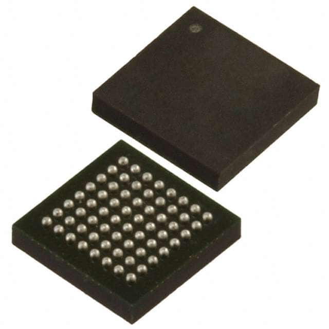
- Small package size: The LCMXO2-256HC-6UMG64C is available in a compact 64-pin Micro FinePitch Ball Grid Array (uFBGA) package.
Packaging/Quantity
The LCMXO2-256HC-6UMG64C is typically packaged in reels or trays. Each reel contains 250 units, while each tray holds 1000 units.
Specifications
- Logic Elements: 256
- Look-Up Tables (LUTs): 1280
- Flip-Flops: 512
- Block RAM: 64 Kbits
- Maximum User I/Os: 49
- Operating Voltage: 1.2V
- Speed Grade: -6
- Package Type: uFBGA
- Package Pins: 64
Detailed Pin Configuration
The LCMXO2-256HC-6UMG64C has a total of 64 pins. The pin configuration is as follows:
(Pin Number) (Pin Name) 1. VCCIO 2. GND 3. IO0 4. IO1 5. IO2 6. IO3 7. IO4 8. IO5 9. IO6 10. IO7 11. IO8 12. IO9 13. IO10 14. IO11 15. IO12 16. IO13 17. IO14 18. IO15 19. IO16 20. IO17 21. IO18 22. IO19 23. IO20 24. IO21 25. IO22 26. IO23 27. IO24 28. IO25 29. IO26 30. IO27 31. IO28 32. IO29 33. IO30 34. IO31 35. IO32 36. IO33 37. IO34 38. IO35 39. IO36 40. IO37 41. IO38 42. IO39 43. IO40 44. IO41 45. IO42 46. IO43 47. IO44 48. IO45 49. IO46 50. IO47 51. IO48 52. IO49 53. GND 54. VCCIO 55. GND 56. VCCIO 57. GND 58. VCCIO 59. GND 60. VCCIO 61. GND 62. VCCIO 63. GND 64. VCCIO
Functional Features
- High-speed performance: The LCMXO2-256HC-6UMG64C offers fast signal processing capabilities, making it suitable for applications requiring real-time data processing.
- Flexible reprogrammability: The FPGA can be easily reconfigured to adapt to changing design requirements without the need for hardware modifications.
- Integrated memory blocks: The built-in Block RAM allows for efficient storage and retrieval of data within the FPGA.
Advantages and Disadvantages
Advantages
- High-performance capabilities
- Low power consumption
- Compact package size
- Flexible reprogrammability
Disadvantages
- Limited number of user I/Os
- Relatively small logic capacity compared to larger FPGAs
Working Principles
The LCMXO2-256HC-6UMG64C operates based on the principles of configurable logic. It consists of a matrix of programmable logic elements interconnected by configurable routing resources. These logic elements can be programmed to perform various digital functions, allowing for the implementation of complex designs.
Detailed Application Field Plans
The LCMXO2-256HC-6UMG64C finds applications in various fields, including: 1.
Seznam 10 běžných otázek a odpovědí souvisejících s aplikací LCMXO2-256HC-6UMG64C v technických řešeních
Sure! Here are 10 common questions and answers related to the application of LCMXO2-256HC-6UMG64C in technical solutions:
Q: What is the LCMXO2-256HC-6UMG64C? A: The LCMXO2-256HC-6UMG64C is a low-cost, low-power FPGA (Field-Programmable Gate Array) device manufactured by Lattice Semiconductor.
Q: What are the key features of the LCMXO2-256HC-6UMG64C? A: Some key features include 256 LUTs (Look-Up Tables), 6400 flip-flops, 64 user I/O pins, 64 macrocells, and support for various I/O standards.
Q: What are some typical applications of the LCMXO2-256HC-6UMG64C? A: The LCMXO2-256HC-6UMG64C is commonly used in applications such as industrial control systems, consumer electronics, communication devices, and automotive systems.
Q: How can I program the LCMXO2-256HC-6UMG64C? A: The LCMXO2-256HC-6UMG64C can be programmed using Lattice Diamond or Lattice Radiant software tools, which provide a graphical interface for designing and programming the FPGA.
Q: What voltage levels does the LCMXO2-256HC-6UMG64C support? A: The LCMXO2-256HC-6UMG64C supports both 3.3V and 1.2V voltage levels, allowing for compatibility with a wide range of external devices.
Q: Can I use the LCMXO2-256HC-6UMG64C in battery-powered applications? A: Yes, the LCMXO2-256HC-6UMG64C is designed to be low-power and can be used in battery-powered applications where power consumption is a concern.
Q: Does the LCMXO2-256HC-6UMG64C support external memory interfaces? A: Yes, the LCMXO2-256HC-6UMG64C supports various memory interfaces such as SPI, I2C, and UART, allowing for easy integration with external memory devices.
Q: Can I reprogram the LCMXO2-256HC-6UMG64C in the field? A: Yes, the LCMXO2-256HC-6UMG64C supports in-system programming (ISP), which allows for reprogramming of the FPGA without the need for physical access to the device.
Q: Are there any development boards available for the LCMXO2-256HC-6UMG64C? A: Yes, Lattice Semiconductor provides development boards specifically designed for the LCMXO2-256HC-6UMG64C, which include all the necessary components for prototyping and testing.
Q: Where can I find more information about the LCMXO2-256HC-6UMG64C? A: You can find more detailed information about the LCMXO2-256HC-6UMG64C, including datasheets, application notes, and reference designs, on the official Lattice Semiconductor website or by contacting their technical support team.