

Viz Specifikace pro podrobnosti o produktu.
LCMXO2-256ZE-2UMG64I
Product Overview
Category
The LCMXO2-256ZE-2UMG64I belongs to the category of Field-Programmable Gate Arrays (FPGAs).
Use
FPGAs are integrated circuits that can be programmed or reprogrammed after manufacturing. The LCMXO2-256ZE-2UMG64I is specifically designed for digital logic applications.
Characteristics
- Low power consumption
- Small form factor
- High performance
- Flexible and customizable
Package
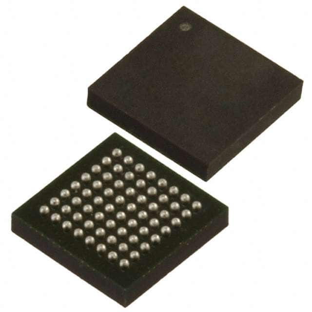
The LCMXO2-256ZE-2UMG64I comes in a compact 64-pin Micro FineLine BGA package.
Essence
The essence of the LCMXO2-256ZE-2UMG64I lies in its ability to provide a versatile platform for implementing complex digital designs.
Packaging/Quantity
The LCMXO2-256ZE-2UMG64I is typically sold individually, and the quantity may vary depending on the supplier.
Specifications
- Logic Cells: 256
- Look-Up Tables (LUTs): 1280
- Flip-Flops: 512
- Block RAM: 64 Kbits
- Maximum Operating Frequency: 100 MHz
- I/O Pins: 48
- Voltage Range: 1.2V - 3.3V
- Configuration Memory: Flash-based
Detailed Pin Configuration
The LCMXO2-256ZE-2UMG64I has a total of 64 pins, each serving a specific purpose. Here is a brief overview of some important pin functions:
- VCCIO: Power supply voltage for input/output buffers.
- GND: Ground reference.
- JTAG: Pins used for Joint Test Action Group (JTAG) boundary scan testing and programming.
- I/O Pins: General-purpose input/output pins for connecting external devices.
- Configuration Pins: Pins used for configuring the FPGA.
For a complete pin configuration diagram, please refer to the manufacturer's datasheet.
Functional Features
The LCMXO2-256ZE-2UMG64I offers several functional features that make it suitable for various applications:
- Programmable Logic: The FPGA can be configured to implement custom digital logic functions.
- Embedded Memory: The built-in Block RAM provides on-chip memory storage.
- Clock Management: The device supports clock multiplication, division, and phase shifting.
- I/O Interfaces: The FPGA offers flexible I/O options for interfacing with external devices.
- Low Power Consumption: The LCMXO2-256ZE-2UMG64I is designed to operate efficiently with low power consumption.
Advantages and Disadvantages
Advantages
- Versatility: The FPGA's programmability allows for a wide range of applications.
- Customizability: Users can tailor the functionality of the FPGA to their specific needs.
- Compact Size: The small form factor makes it suitable for space-constrained designs.
- High Performance: The LCMXO2-256ZE-2UMG64I offers fast processing speeds and low latency.
Disadvantages
- Complexity: Programming and configuring FPGAs require specialized knowledge and expertise.
- Cost: FPGAs can be more expensive compared to other integrated circuits.
- Limited Resources: The number of logic cells and memory capacity may not be sufficient for highly complex designs.
Working Principles
FPGAs like the LCMXO2-256ZE-2UMG64I consist of an array of configurable logic blocks interconnected by programmable routing channels. These logic blocks can be programmed to perform specific functions using Hardware Description Languages (HDLs) such as VHDL or Verilog. The configuration data is stored in the on-chip flash memory and loaded during startup.
Once programmed, the FPGA operates based on the logic implemented within its fabric. Input signals are processed through the configurable logic blocks, and the output is routed to the desired destination using the programmable routing channels. This flexibility allows for the implementation of complex digital systems on a single chip.
Detailed Application Field Plans
The LCMXO2-256ZE-2UMG64I finds applications in various fields, including:
- Communications: Used in wireless communication systems for signal processing and protocol implementation.
- Industrial Automation: Employed in control systems for process monitoring and automation.
- Consumer Electronics: Integrated into multimedia devices, gaming consoles, and smart home appliances.
- Automotive: Utilized in automotive electronics for engine control, infotainment systems, and driver assistance.
- Aerospace: Used in avionics systems for navigation, communication, and flight control.
These are just a few examples, and the versatility of FPGAs allows them to be applied in many other domains.
Detailed and Complete Alternative Models
- L
Seznam 10 běžných otázek a odpovědí souvisejících s aplikací LCMXO2-256ZE-2UMG64I v technických řešeních
Sure! Here are 10 common questions and answers related to the application of LCMXO2-256ZE-2UMG64I in technical solutions:
Q: What is the LCMXO2-256ZE-2UMG64I? A: The LCMXO2-256ZE-2UMG64I is a low-cost, low-power FPGA (Field-Programmable Gate Array) device manufactured by Lattice Semiconductor.
Q: What are the key features of the LCMXO2-256ZE-2UMG64I? A: Some key features include 256 Look-Up Tables (LUTs), 2,560 programmable logic cells, 64 I/O pins, and support for various I/O standards.
Q: What are some typical applications of the LCMXO2-256ZE-2UMG64I? A: The LCMXO2-256ZE-2UMG64I is commonly used in applications such as industrial control systems, consumer electronics, medical devices, and communication equipment.
Q: How can I program the LCMXO2-256ZE-2UMG64I? A: The LCMXO2-256ZE-2UMG64I can be programmed using Lattice Diamond or Lattice Radiant software tools, which provide a graphical interface for designing and programming the FPGA.
Q: What voltage levels does the LCMXO2-256ZE-2UMG64I support? A: The LCMXO2-256ZE-2UMG64I supports both 3.3V and 1.2V voltage levels, making it compatible with a wide range of digital systems.
Q: Can I use the LCMXO2-256ZE-2UMG64I in battery-powered applications? A: Yes, the LCMXO2-256ZE-2UMG64I is designed to be low-power and can be used in battery-powered applications where power efficiency is crucial.
Q: Does the LCMXO2-256ZE-2UMG64I have any built-in peripherals? A: No, the LCMXO2-256ZE-2UMG64I does not have any built-in peripherals. However, it can be easily interfaced with external components using its I/O pins.
Q: Can I reprogram the LCMXO2-256ZE-2UMG64I multiple times? A: Yes, the LCMXO2-256ZE-2UMG64I is a reprogrammable FPGA, allowing you to modify and reconfigure its functionality as needed.
Q: What development boards or evaluation kits are available for the LCMXO2-256ZE-2UMG64I? A: Lattice Semiconductor offers various development boards and evaluation kits specifically designed for the LCMXO2-256ZE-2UMG64I, such as the iCE40 UltraPlus Breakout Board.
Q: Are there any online resources or communities for support with the LCMXO2-256ZE-2UMG64I? A: Yes, Lattice Semiconductor provides documentation, application notes, and a community forum where users can seek help and share knowledge about their LCMXO2-256ZE-2UMG64I projects.
Please note that the answers provided here are general and may vary depending on specific requirements and use cases.