

Viz Specifikace pro podrobnosti o produktu.
LCMXO2-256ZE-3SG32C
Product Overview
Category
The LCMXO2-256ZE-3SG32C belongs to the category of Field Programmable Gate Arrays (FPGAs).
Use
FPGAs are integrated circuits that can be programmed and reprogrammed to perform various digital functions. The LCMXO2-256ZE-3SG32C is specifically designed for applications requiring low power consumption and small form factor.
Characteristics
- Low power consumption
- Small form factor
- High performance
- Flexible and reprogrammable
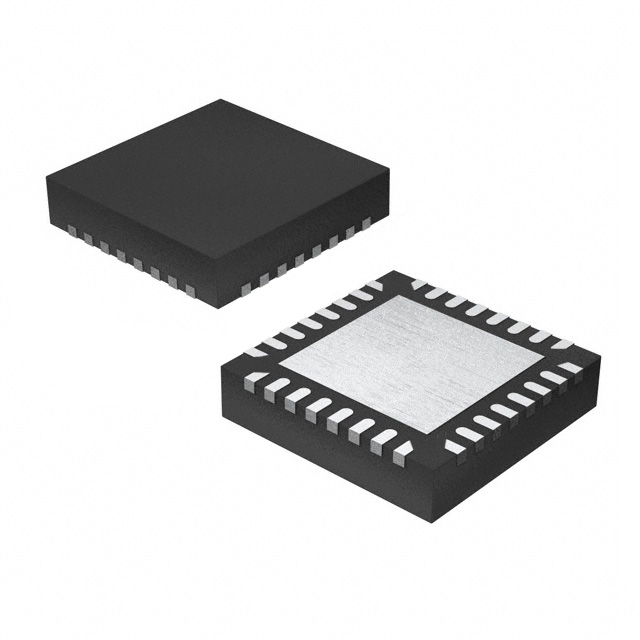
Package
The LCMXO2-256ZE-3SG32C comes in a small form factor package, making it suitable for space-constrained applications.
Essence
The essence of the LCMXO2-256ZE-3SG32C lies in its ability to provide high-performance digital functionality while consuming minimal power and occupying a small footprint.
Packaging/Quantity
The LCMXO2-256ZE-3SG32C is typically packaged in reels or trays, with a quantity of 250 units per reel/tray.
Specifications
- FPGA Family: Lattice XO2
- Logic Elements: 256
- Speed Grade: -3
- Package Type: SG32
- I/O Pins: 32
- Operating Voltage: 1.2V
- Maximum Frequency: 100 MHz
- Configuration Memory: 256 kbits
- Embedded Block RAM: 4.5 kbits
- Power Supply Current: 20 mA
Detailed Pin Configuration
The LCMXO2-256ZE-3SG32C has a total of 32 I/O pins, which are configurable based on the specific application requirements. The pin configuration allows for easy integration into various circuit designs.
Functional Features
- Low power consumption enables energy-efficient operation.
- High-performance logic elements provide fast processing capabilities.
- Reprogrammable nature allows for flexibility and adaptability.
- Small form factor makes it suitable for space-constrained applications.
Advantages and Disadvantages
Advantages
- Low power consumption
- Small form factor
- High performance
- Reprogrammable
Disadvantages
- Limited logic elements compared to larger FPGAs
- Relatively higher cost per logic element
Working Principles
The LCMXO2-256ZE-3SG32C operates based on the principles of digital logic. It consists of configurable logic blocks, interconnects, and I/O pins. The logic blocks can be programmed to perform specific functions, allowing for the implementation of complex digital circuits.
Detailed Application Field Plans
The LCMXO2-256ZE-3SG32C is well-suited for a wide range of applications, including but not limited to: - Internet of Things (IoT) devices - Wearable technology - Embedded systems - Consumer electronics - Industrial automation
Detailed and Complete Alternative Models
- LCMXO2-1200HC-4TG144C
- LCMXO2-7000HE-5TG144C
- LCMXO2-4000HC-6TG144C
- LCMXO2-2000HC-7TG144C
- LCMXO2-640HC-8TG100C
These alternative models offer varying levels of logic elements, speed grades, and package types, providing options to suit different application requirements.
In conclusion, the LCMXO2-256ZE-3SG32C is a low-power, small form factor FPGA that offers high performance and flexibility. Its compact size and reprogrammable nature make it suitable for a wide range of applications in various industries.
Seznam 10 běžných otázek a odpovědí souvisejících s aplikací LCMXO2-256ZE-3SG32C v technických řešeních
Sure! Here are 10 common questions and answers related to the application of LCMXO2-256ZE-3SG32C in technical solutions:
Q: What is the LCMXO2-256ZE-3SG32C? A: The LCMXO2-256ZE-3SG32C is a low-cost, low-power FPGA (Field-Programmable Gate Array) device manufactured by Lattice Semiconductor.
Q: What are the key features of the LCMXO2-256ZE-3SG32C? A: Some key features include 256 Look-Up Tables (LUTs), 2,560 programmable logic cells, 8 multipliers, 4 Phase-Locked Loops (PLLs), and support for various I/O standards.
Q: What are some typical applications of the LCMXO2-256ZE-3SG32C? A: The LCMXO2-256ZE-3SG32C is commonly used in applications such as industrial control systems, consumer electronics, communication devices, and automotive systems.
Q: How can I program the LCMXO2-256ZE-3SG32C? A: The LCMXO2-256ZE-3SG32C can be programmed using Lattice Diamond or Lattice Radiant software tools, which provide a graphical interface for designing and programming the FPGA.
Q: What voltage levels does the LCMXO2-256ZE-3SG32C support? A: The LCMXO2-256ZE-3SG32C supports both 3.3V and 1.2V voltage levels, making it compatible with a wide range of digital systems.
Q: Can I use the LCMXO2-256ZE-3SG32C for high-speed applications? A: While the LCMXO2-256ZE-3SG32C is not specifically designed for high-speed applications, it can still handle moderate-speed designs with proper optimization and careful consideration of timing constraints.
Q: Does the LCMXO2-256ZE-3SG32C have built-in memory? A: No, the LCMXO2-256ZE-3SG32C does not have built-in memory. However, it can interface with external memory devices such as SRAM or Flash memory.
Q: Can I use the LCMXO2-256ZE-3SG32C in battery-powered devices? A: Yes, the LCMXO2-256ZE-3SG32C is known for its low power consumption, making it suitable for battery-powered applications where power efficiency is crucial.
Q: What are some advantages of using the LCMXO2-256ZE-3SG32C over other FPGAs? A: Some advantages include its low cost, low power consumption, small form factor, and ease of use due to the availability of user-friendly software tools.
Q: Where can I find more information about the LCMXO2-256ZE-3SG32C? A: You can find more detailed information about the LCMXO2-256ZE-3SG32C on the official website of Lattice Semiconductor or by referring to the datasheet and application notes provided by the manufacturer.