

Viz Specifikace pro podrobnosti o produktu.
LCMXO2-640HC-4SG48I
Product Overview
Category
The LCMXO2-640HC-4SG48I belongs to the category of Field-Programmable Gate Arrays (FPGAs).
Use
FPGAs are integrated circuits that can be programmed and reprogrammed to perform various digital functions. The LCMXO2-640HC-4SG48I is specifically designed for applications requiring low power consumption and high performance.
Characteristics
- Low power consumption: The LCMXO2-640HC-4SG48I is optimized for low power operation, making it suitable for battery-powered devices.
- High performance: With a high logic density and fast operating speed, this FPGA can handle complex digital designs efficiently.
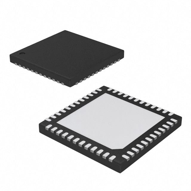
- Small package size: The device comes in a compact 48-pin Small Grid Array (SGA) package, allowing for space-efficient integration into electronic systems.
- Versatile functionality: The LCMXO2-640HC-4SG48I offers a wide range of programmable features, including configurable logic blocks, embedded memory, and I/O interfaces.
Package and Quantity
The LCMXO2-640HC-4SG48I is available in a 48-pin Small Grid Array (SGA) package. It is typically sold individually or in small quantities.
Specifications
- Logic Elements: 640
- Look-Up Tables (LUTs): 1280
- Flip-Flops: 2560
- Block RAM: 64 Kbits
- Maximum Operating Frequency: 100 MHz
- I/O Pins: 36
- Voltage Range: 1.2V - 3.3V
- Package Type: SGA
- Package Dimensions: 7mm x 7mm
Detailed Pin Configuration
The pin configuration of the LCMXO2-640HC-4SG48I is as follows:
- VCCIO
- GND
- IO_0
- IO_1
- IO_2
- IO_3
- IO_4
- IO_5
- IO_6
- IO_7
- IO_8
- IO_9
- IO_10
- IO_11
- IO_12
- IO_13
- IO_14
- IO_15
- IO_16
- IO_17
- IO_18
- IO_19
- IO_20
- IO_21
- IO_22
- IO_23
- IO_24
- IO_25
- IO_26
- IO_27
- IO_28
- IO_29
- IO_30
- IO_31
- IO_32
- IO_33
- IO_34
- IO_35
- GND
- VCCIO
Functional Features
The LCMXO2-640HC-4SG48I offers the following functional features:
- Configurable Logic Blocks (CLBs): These blocks can be programmed to implement various digital functions, such as combinational logic, arithmetic operations, and state machines.
- Embedded Memory: The FPGA includes built-in memory blocks that can be used for data storage or as lookup tables.
- I/O Interfaces: The device provides multiple I/O pins for connecting to external devices, enabling communication and data transfer.
- Clock Management: The FPGA supports clock signals for synchronizing internal operations and interfacing with external systems.
Advantages and Disadvantages
Advantages
- Low power consumption makes it suitable for battery-powered devices.
- High logic density and fast operating speed enable efficient handling of complex designs.
- Versatile functionality allows for a wide range of applications.
- Small package size enables space-efficient integration.
Disadvantages
- Limited number of I/O pins may restrict connectivity options in certain applications.
- Programming and configuring FPGAs can be complex and time-consuming for inexperienced users.
Working Principles
The LCMXO2-640HC-4SG48I operates based on the principles of reconfigurable digital logic. It consists of configurable logic blocks, memory elements, and I/O interfaces. The device can be programmed using hardware description languages (HDL) or graphical design tools to define the desired digital circuitry. Once programmed, the FPGA executes the specified logic functions and performs the required operations.
Detailed Application Field Plans
The LCMXO2-640HC-4SG48I is well-suited for various applications, including:
- Embedded Systems: The FPGA can be used to implement control and communication functions in embedded systems, such as industrial
Seznam 10 běžných otázek a odpovědí souvisejících s aplikací LCMXO2-640HC-4SG48I v technických řešeních
Sure! Here are 10 common questions and answers related to the application of LCMXO2-640HC-4SG48I in technical solutions:
Q: What is the LCMXO2-640HC-4SG48I? A: The LCMXO2-640HC-4SG48I is a low-cost, low-power FPGA (Field-Programmable Gate Array) device manufactured by Lattice Semiconductor.
Q: What are the key features of LCMXO2-640HC-4SG48I? A: The key features include 640 Look-Up Tables (LUTs), 8Kbits of embedded memory, 34 I/O pins, low power consumption, and small form factor.
Q: What are some typical applications of LCMXO2-640HC-4SG48I? A: It is commonly used in applications such as industrial automation, consumer electronics, medical devices, communication systems, and IoT (Internet of Things) devices.
Q: How can I program the LCMXO2-640HC-4SG48I? A: You can program the device using Lattice Diamond or Lattice Radiant software tools, which support various programming languages like VHDL and Verilog.
Q: What is the power supply requirement for LCMXO2-640HC-4SG48I? A: The device operates at a voltage range of 1.14V to 3.465V, with a recommended operating voltage of 1.2V.
Q: Can I use LCMXO2-640HC-4SG48I for high-speed applications? A: While the device is not specifically designed for high-speed applications, it can still handle moderate-speed designs depending on the specific requirements.
Q: Does LCMXO2-640HC-4SG48I support external memory interfaces? A: Yes, it supports various external memory interfaces like SPI (Serial Peripheral Interface) and I2C (Inter-Integrated Circuit).
Q: Can I use LCMXO2-640HC-4SG48I for real-time signal processing? A: Yes, the device can be used for real-time signal processing applications by implementing appropriate algorithms in the FPGA fabric.
Q: What are the advantages of using LCMXO2-640HC-4SG48I over other FPGAs? A: The advantages include low cost, low power consumption, small form factor, and ease of programming using Lattice's software tools.
Q: Where can I find more technical documentation and support for LCMXO2-640HC-4SG48I? A: You can visit the official website of Lattice Semiconductor or refer to their datasheets, application notes, and user guides for detailed technical information. Additionally, Lattice provides customer support through their online forums and technical support channels.