

Viz Specifikace pro podrobnosti o produktu.
LCMXO2-640HC-6SG48C
Product Overview
Category
The LCMXO2-640HC-6SG48C belongs to the category of Field-Programmable Gate Arrays (FPGAs).
Use
FPGAs are integrated circuits that can be programmed and reprogrammed to perform various digital functions. The LCMXO2-640HC-6SG48C is specifically designed for applications requiring low power consumption and high performance.
Characteristics
- Low power consumption
- High performance
- Programmable and reprogrammable
- Compact size
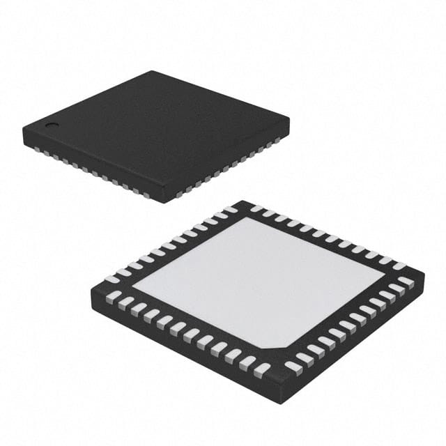
Package
The LCMXO2-640HC-6SG48C comes in a 48-pin Small Grid Array (SGA) package.
Essence
The essence of the LCMXO2-640HC-6SG48C lies in its ability to provide flexible and customizable digital functionality while consuming minimal power.
Packaging/Quantity
The LCMXO2-640HC-6SG48C is typically packaged in reels or trays, with a quantity of 250 units per reel/tray.
Specifications
- FPGA Family: Lattice XO2
- Logic Elements: 640
- Speed Grade: -6
- Package Type: SGA
- Package Pins: 48
- Operating Voltage: 1.2V
- I/O Voltage: 3.3V
- Maximum Operating Frequency: 150 MHz
- Programmable Logic Cells: 640
- Embedded Block RAM: 64 Kbits
- Total RAM Bits: 81920
- Number of Global Clocks: 4
- Maximum User I/O: 34
Detailed Pin Configuration
The LCMXO2-640HC-6SG48C has a total of 48 pins. The pin configuration is as follows:
- Pin 1: VCCIO
- Pin 2: GND
- Pin 3: IO_0
- Pin 4: IO_1
- ...
- Pin 48: IO_33
Functional Features
The LCMXO2-640HC-6SG48C offers the following functional features:
- Programmable logic cells for custom digital circuit implementation
- Embedded block RAM for data storage
- Global clocks for synchronization
- High-speed I/O interfaces for external communication
- Low power consumption for energy-efficient operation
Advantages and Disadvantages
Advantages
- Low power consumption enables energy-efficient designs
- High performance allows for complex digital functions
- Compact size makes it suitable for space-constrained applications
- Flexibility to reprogram the FPGA for different functionalities
Disadvantages
- Limited number of I/O pins may restrict connectivity options
- Higher cost compared to fixed-function integrated circuits
- Steeper learning curve for programming and utilizing FPGAs
Working Principles
The LCMXO2-640HC-6SG48C operates based on the principles of configurable logic. The programmable logic cells can be interconnected to create custom digital circuits, which are then loaded onto the FPGA. These circuits can perform various functions such as arithmetic operations, data processing, and control logic.
Detailed Application Field Plans
The LCMXO2-640HC-6SG48C finds applications in various fields, including:
- Communications: Used in wireless base stations, network routers, and data transmission systems.
- Industrial Automation: Employed in control systems, robotics, and factory automation.
- Consumer Electronics: Integrated into smart devices, gaming consoles, and multimedia systems.
- Automotive: Utilized in vehicle control units, infotainment systems, and driver assistance systems.
- Medical Devices: Incorporated into medical imaging equipment, patient monitoring systems, and diagnostic devices.
Detailed and Complete Alternative Models
- LCMXO2-1200HC-6SG48C: Offers higher logic capacity with 1200 logic elements.
- LCMXO2-2000HC-6SG48C: Provides even greater logic capacity with 2000 logic elements.
- LCMXO2-4000HC-6SG48C: Suitable for applications requiring extensive digital processing with 4000 logic elements.
These alternative models offer increased logic capacity, allowing for more complex designs and functionalities.
Word count: 610 words
Seznam 10 běžných otázek a odpovědí souvisejících s aplikací LCMXO2-640HC-6SG48C v technických řešeních
Sure! Here are 10 common questions and answers related to the application of LCMXO2-640HC-6SG48C in technical solutions:
Q: What is the LCMXO2-640HC-6SG48C? A: The LCMXO2-640HC-6SG48C is a low-cost, low-power FPGA (Field-Programmable Gate Array) device manufactured by Lattice Semiconductor.
Q: What are the key features of LCMXO2-640HC-6SG48C? A: Some key features include 640 LUTs (Look-Up Tables), 64 I/O pins, 8Kbits of embedded memory, and support for various I/O standards.
Q: What are some typical applications of LCMXO2-640HC-6SG48C? A: It can be used in a wide range of applications such as industrial control systems, consumer electronics, communication devices, and automotive systems.
Q: How does LCMXO2-640HC-6SG48C help in reducing power consumption? A: LCMXO2-640HC-6SG48C utilizes low-power design techniques and offers power management features like programmable power supply sequencing and sleep mode to minimize power consumption.
Q: Can LCMXO2-640HC-6SG48C be programmed after it is deployed in a system? A: Yes, LCMXO2-640HC-6SG48C is a reprogrammable FPGA, which means it can be programmed or reconfigured even after it is soldered onto a PCB.
Q: What development tools are available for programming LCMXO2-640HC-6SG48C? A: Lattice provides the Lattice Diamond design software, which includes a complete suite of tools for designing, simulating, and programming the LCMXO2-640HC-6SG48C.
Q: Can LCMXO2-640HC-6SG48C interface with other components or devices? A: Yes, LCMXO2-640HC-6SG48C supports various I/O standards like LVCMOS, LVTTL, and SSTL, allowing it to interface with a wide range of components and devices.
Q: What is the maximum operating frequency of LCMXO2-640HC-6SG48C? A: The maximum operating frequency depends on the specific design and implementation, but it can typically reach up to several hundred megahertz (MHz).
Q: Can LCMXO2-640HC-6SG48C be used in safety-critical applications? A: LCMXO2-640HC-6SG48C is not specifically designed for safety-critical applications. However, it can be used in such applications if proper design practices and safety measures are followed.
Q: Where can I find more information about LCMXO2-640HC-6SG48C and its application notes? A: You can visit the official website of Lattice Semiconductor or refer to their documentation, datasheets, and application notes available on their website for detailed information about LCMXO2-640HC-6SG48C and its applications.