

Viz Specifikace pro podrobnosti o produktu.
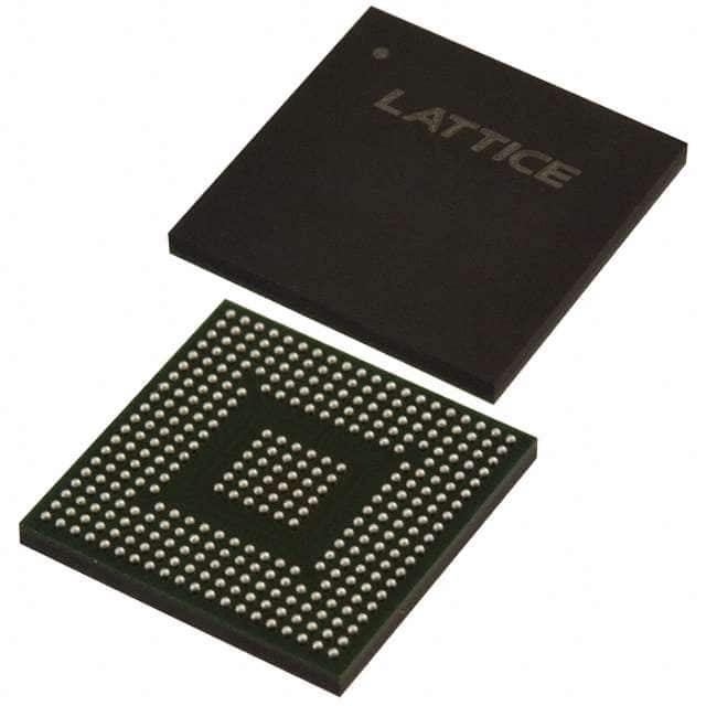
LCMXO2-7000HC-4BG332C
Product Overview
Category
The LCMXO2-7000HC-4BG332C belongs to the category of Field-Programmable Gate Arrays (FPGAs).
Use
FPGAs are integrated circuits that can be programmed after manufacturing, allowing for flexible and customizable digital logic designs. The LCMXO2-7000HC-4BG332C is specifically designed for applications requiring low power consumption and high performance.
Characteristics
- Low power consumption: The LCMXO2-7000HC-4BG332C is optimized for low power operation, making it suitable for battery-powered devices.
- High performance: With a high-speed programmable fabric, this FPGA offers excellent performance for various applications.
- Small package size: The LCMXO2-7000HC-4BG332C comes in a compact package, making it suitable for space-constrained designs.
- High reliability: This FPGA is built with robust materials and undergoes rigorous testing to ensure reliable operation.
Package and Quantity
The LCMXO2-7000HC-4BG332C is available in a 332-ball grid array (BGA) package. It is typically sold individually or in small quantities.
Specifications
- Logic Elements: 7,000
- Look-Up Tables (LUTs): 4,500
- Flip-Flops: 9,000
- Block RAM: 270 Kbits
- Maximum User I/Os: 332
- Operating Voltage: 1.2V
- Speed Grade: -4
Pin Configuration
The LCMXO2-7000HC-4BG332C has a total of 332 pins, each serving a specific function within the FPGA. The pin configuration varies depending on the application and design requirements. Please refer to the manufacturer's datasheet for detailed pin assignments.
Functional Features
- Programmability: The LCMXO2-7000HC-4BG332C offers reprogrammable logic, allowing users to modify the functionality of the FPGA as needed.
- Low Power Consumption: This FPGA is designed to operate efficiently with minimal power consumption, making it suitable for battery-powered devices.
- High-Speed Performance: With its high-speed programmable fabric, the LCMXO2-7000HC-4BG332C delivers excellent performance for demanding applications.
- Flexible I/O Options: The FPGA provides a wide range of user I/Os, enabling connectivity with various external devices and interfaces.
- Embedded Memory: The built-in block RAM allows for efficient data storage and retrieval within the FPGA.
Advantages and Disadvantages
Advantages
- Flexibility: FPGAs offer the advantage of being highly flexible and customizable, allowing for rapid prototyping and design iterations.
- Low Development Cost: Compared to application-specific integrated circuits (ASICs), FPGAs have lower development costs due to their reprogrammability.
- Time-to-Market: FPGAs enable faster time-to-market as they eliminate the need for custom chip fabrication.
- Power Efficiency: The LCMXO2-7000HC-4BG332C is optimized for low power consumption, making it suitable for energy-efficient designs.
Disadvantages
- Complexity: Designing with FPGAs requires specialized knowledge and expertise, which may pose challenges for inexperienced users.
- Limited Resources: FPGAs have finite resources, such as logic elements and memory, which may restrict the complexity of designs.
- Higher Cost per Unit: FPGAs generally have a higher cost per unit compared to mass-produced ASICs.
Working Principles
FPGAs consist of an array of configurable logic blocks (CLBs) interconnected through programmable routing resources. The LCMXO2-7000HC-4BG332C utilizes lookup tables (LUTs) to implement digital logic functions and flip-flops for sequential circuit elements. These components can be programmed using hardware description languages (HDLs) or graphical design tools.
The FPGA's configuration is stored in non-volatile memory, allowing it to retain the programmed functionality even after power is removed. During operation, the FPGA executes the user-defined logic based on the programmed configuration, enabling the desired functionality.
Application Field Plans
The LCMXO2-7000HC-4BG332C finds applications in various fields, including:
- Embedded Systems: The FPGA can be used to implement custom interfaces, control systems, and signal processing algorithms in embedded systems.
- Communications: It can be utilized in networking equipment, such as routers and switches, to handle high-speed data processing and protocol conversions.
- Industrial Automation: FPGAs enable the implementation of real-time control systems, motor control, and sensor interfacing in industrial automation applications.
- Medical Devices: The FPGA can
Seznam 10 běžných otázek a odpovědí souvisejících s aplikací LCMXO2-7000HC-4BG332C v technických řešeních
Sure! Here are 10 common questions and answers related to the application of LCMXO2-7000HC-4BG332C in technical solutions:
Q: What is the LCMXO2-7000HC-4BG332C? A: The LCMXO2-7000HC-4BG332C is a low-cost, low-power FPGA (Field-Programmable Gate Array) device manufactured by Lattice Semiconductor.
Q: What are the key features of LCMXO2-7000HC-4BG332C? A: Some key features include 7000 Look-Up Tables (LUTs), 128 Kbits of embedded block RAM, 58 I/O pins, and support for various I/O standards.
Q: What are some typical applications of LCMXO2-7000HC-4BG332C? A: It can be used in a wide range of applications such as industrial automation, consumer electronics, medical devices, communication systems, and more.
Q: How can I program the LCMXO2-7000HC-4BG332C? A: You can program the device using Lattice Diamond design software or iCEcube2 software, which provide a graphical interface for designing and programming the FPGA.
Q: Can I reprogram the LCMXO2-7000HC-4BG332C after it has been programmed once? A: Yes, the LCMXO2-7000HC-4BG332C is a reprogrammable device, allowing you to modify the configuration and functionality as needed.
Q: What power supply voltage does the LCMXO2-7000HC-4BG332C require? A: The device operates at a nominal voltage of 3.3V, but it also supports a wide range of input voltages from 2.375V to 3.63V.
Q: Can I interface the LCMXO2-7000HC-4BG332C with other components or microcontrollers? A: Yes, the device has multiple I/O pins that can be used to interface with other components or microcontrollers using various communication protocols such as SPI, I2C, UART, etc.
Q: What is the maximum operating frequency of the LCMXO2-7000HC-4BG332C? A: The maximum operating frequency depends on the design and implementation, but it can typically reach frequencies of up to 150 MHz.
Q: Are there any development boards available for prototyping with the LCMXO2-7000HC-4BG332C? A: Yes, Lattice Semiconductor provides development boards like the iCE40-HX8K Breakout Board, which includes the LCMXO2-7000HC-4BG332C FPGA.
Q: Where can I find more resources and documentation for the LCMXO2-7000HC-4BG332C? A: You can visit the official Lattice Semiconductor website, where you will find datasheets, application notes, reference designs, and other helpful resources for the LCMXO2-7000HC-4BG332C.