

Viz Specifikace pro podrobnosti o produktu.
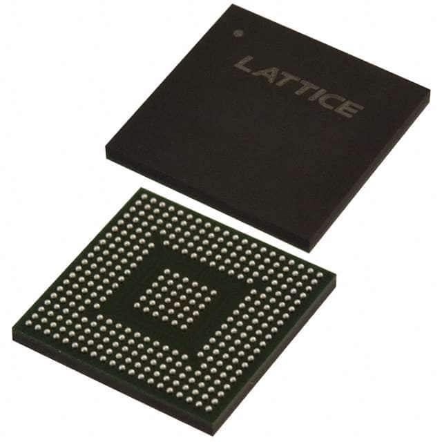
LCMXO2-7000ZE-1BG332C
Product Overview
Category
The LCMXO2-7000ZE-1BG332C belongs to the category of Field Programmable Gate Arrays (FPGAs).
Use
FPGAs are integrated circuits that can be programmed and reprogrammed to perform various digital functions. The LCMXO2-7000ZE-1BG332C is specifically designed for applications requiring low power consumption and high performance.
Characteristics
- Low power consumption: The LCMXO2-7000ZE-1BG332C is optimized for low power operation, making it suitable for battery-powered devices.
- High performance: With a large number of logic elements and built-in memory blocks, this FPGA offers high-speed processing capabilities.
- Small package size: The device comes in a compact package, allowing for space-efficient designs.
- Versatile I/O options: The LCMXO2-7000ZE-1BG332C provides a wide range of input/output options, enabling connectivity with other components.
Package and Quantity
The LCMXO2-7000ZE-1BG332C is available in a 332-ball FineLine BGA package. It is typically sold individually or in small quantities.
Specifications
- Logic Elements: 7,000
- Look-Up Tables (LUTs): 4,500
- Flip-Flops: 9,000
- Block RAM: 270 Kbits
- Maximum User I/Os: 332
- Operating Voltage: 1.2V
- Operating Temperature Range: -40°C to 85°C
Pin Configuration
The detailed pin configuration of the LCMXO2-7000ZE-1BG332C can be found in the product datasheet provided by the manufacturer.
Functional Features
- Programmability: The LCMXO2-7000ZE-1BG332C can be programmed using Hardware Description Languages (HDL) such as VHDL or Verilog, allowing for flexible and customizable designs.
- Reconfigurability: FPGAs can be reprogrammed multiple times, making them suitable for prototyping and iterative development processes.
- High-speed processing: The FPGA's architecture enables fast data processing and parallel execution of tasks.
- Integration capabilities: The LCMXO2-7000ZE-1BG332C can integrate various digital functions into a single chip, reducing the need for additional components.
Advantages and Disadvantages
Advantages
- Low power consumption makes it ideal for battery-powered devices.
- Versatile I/O options allow for easy integration with other components.
- Compact package size enables space-efficient designs.
- High-performance capabilities enable complex digital processing tasks.
Disadvantages
- Limited logic elements compared to higher-end FPGAs.
- May require expertise in HDL programming for optimal utilization.
- Higher cost compared to traditional microcontrollers for simple applications.
Working Principles
FPGAs consist of an array of configurable logic blocks interconnected by programmable routing channels. The LCMXO2-7000ZE-1BG332C utilizes look-up tables and flip-flops to implement desired logic functions. These functions are defined through HDL programming, which configures the interconnections between logic blocks.
During operation, the FPGA executes the programmed logic functions in parallel, providing high-speed processing capabilities. The reconfigurable nature of FPGAs allows for flexibility in modifying the design and adapting to changing requirements.
Application Field Plans
The LCMXO2-7000ZE-1BG332C finds applications in various fields, including:
- Embedded Systems: It can be used in embedded systems for controlling and interfacing with peripheral devices.
- Communications: The FPGA's high-speed processing capabilities make it suitable for data communication applications, such as network routers and switches.
- Industrial Automation: It can be employed in industrial automation systems for real-time control and monitoring.
- Medical Devices: The FPGA's low power consumption and reconfigurability make it useful in medical devices, such as portable diagnostic equipment.
Alternative Models
- LCMXO2-1200ZE-1BG256C
- LCMXO2-2000HC-4TG144C
- LCMXO2-4000HE-5MG132C
These alternative models offer different logic element counts, I/O options, and package sizes, providing flexibility to suit specific project requirements.
In conclusion, the LCMXO2-7000ZE-1BG332C is a versatile FPGA with low power consumption, high performance, and compact size. Its programmability, reconfigurability, and integration capabilities make it suitable for a wide range of applications in various industries.
Seznam 10 běžných otázek a odpovědí souvisejících s aplikací LCMXO2-7000ZE-1BG332C v technických řešeních
Sure! Here are 10 common questions and answers related to the application of LCMXO2-7000ZE-1BG332C in technical solutions:
Q1: What is the LCMXO2-7000ZE-1BG332C? A1: The LCMXO2-7000ZE-1BG332C is a low-cost, low-power FPGA (Field-Programmable Gate Array) device manufactured by Lattice Semiconductor.
Q2: What are the key features of LCMXO2-7000ZE-1BG332C? A2: Some key features of LCMXO2-7000ZE-1BG332C include 7000 Look-Up Tables (LUTs), 128 Kbits of embedded block RAM, 58 I/O pins, and support for various I/O standards.
Q3: What are some typical applications of LCMXO2-7000ZE-1BG332C? A3: LCMXO2-7000ZE-1BG332C is commonly used in applications such as industrial automation, consumer electronics, communication systems, and IoT devices.
Q4: How can I program the LCMXO2-7000ZE-1BG332C? A4: The LCMXO2-7000ZE-1BG332C can be programmed using Lattice Diamond or Lattice Radiant software tools, which provide a graphical interface for designing and programming the FPGA.
Q5: What is the power consumption of LCMXO2-7000ZE-1BG332C? A5: The power consumption of LCMXO2-7000ZE-1BG332C depends on the design and operating conditions but is generally low due to its low-power architecture.
Q6: Can I use LCMXO2-7000ZE-1BG332C for high-speed applications? A6: While LCMXO2-7000ZE-1BG332C is not specifically designed for high-speed applications, it can still handle moderate-speed designs with proper considerations.
Q7: Does LCMXO2-7000ZE-1BG332C support external memory interfaces? A7: Yes, LCMXO2-7000ZE-1BG332C supports various external memory interfaces such as SPI, I2C, and UART, allowing for easy integration with other devices.
Q8: Can I reprogram the LCMXO2-7000ZE-1BG332C in the field? A8: Yes, LCMXO2-7000ZE-1BG332C supports in-system programming (ISP), which allows you to reprogram the FPGA without removing it from the system.
Q9: What are the temperature specifications of LCMXO2-7000ZE-1BG332C? A9: The operating temperature range for LCMXO2-7000ZE-1BG332C is typically -40°C to 85°C, making it suitable for a wide range of environments.
Q10: Are there any development boards available for LCMXO2-7000ZE-1BG332C? A10: Yes, Lattice Semiconductor offers development boards like the LCMXO2-7000ZE-B-EVN, which provide a platform for prototyping and testing designs using this FPGA.
Please note that these answers are general and may vary depending on specific requirements and design considerations.