

Viz Specifikace pro podrobnosti o produktu.
LCMXO3L-640E-6MG121I
Product Overview
Category
The LCMXO3L-640E-6MG121I belongs to the category of Field Programmable Gate Arrays (FPGAs).
Use
This FPGA is commonly used in electronic design and prototyping applications, where it provides a flexible and reconfigurable platform for implementing digital logic circuits.
Characteristics
- High-performance FPGA with low power consumption
- Compact package size
- Wide range of I/O interfaces
- Configurable logic blocks for custom circuit implementation
- On-chip memory resources for data storage
- Support for various communication protocols
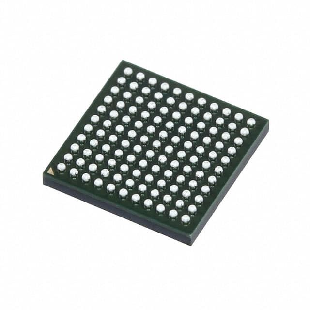
Package
The LCMXO3L-640E-6MG121I is available in a small form factor package, making it suitable for space-constrained designs.
Essence
The essence of this FPGA lies in its ability to be programmed and reprogrammed to perform different functions, allowing for rapid development and testing of complex digital systems.
Packaging/Quantity
The LCMXO3L-640E-6MG121I is typically sold individually or in small quantities, depending on the supplier.
Specifications
- Logic Elements: 640 LUTs (Look-Up Tables)
- Embedded Memory: 4.5 Kbits
- Maximum User I/Os: 121
- Operating Voltage: 1.2V
- Speed Grade: 6
- Package Type: MG121
Detailed Pin Configuration
The pin configuration of the LCMXO3L-640E-6MG121I FPGA is as follows:
- Pin 1: VCCIO
- Pin 2: GND
- Pin 3: IO0
- Pin 4: IO1
- ...
- Pin 121: IO120
Please refer to the datasheet for a complete pinout diagram.
Functional Features
- Configurable logic blocks for implementing custom digital circuits
- Dedicated hardware multipliers for efficient arithmetic operations
- On-chip memory resources for data storage and retrieval
- Flexible I/O interfaces for connecting to external devices
- Support for various communication protocols, such as SPI, I2C, UART, etc.
- Clock management resources for precise timing control
Advantages and Disadvantages
Advantages
- High-performance FPGA with low power consumption
- Compact package size suitable for space-constrained designs
- Reconfigurable nature allows for rapid prototyping and development
- Wide range of I/O interfaces for versatile connectivity options
- Support for various communication protocols enhances compatibility
Disadvantages
- Limited logic elements and memory compared to larger FPGAs
- Higher cost per logic element compared to other programmable logic devices
- Steeper learning curve for beginners due to the complexity of FPGA programming
Working Principles
The LCMXO3L-640E-6MG121I FPGA operates based on the principles of configurable logic. It consists of a matrix of configurable logic blocks (CLBs) interconnected through programmable routing resources. The CLBs can be programmed to implement desired digital logic functions using Look-Up Tables (LUTs) and flip-flops. The interconnections between CLBs are established by configuring the routing resources, allowing for the creation of complex digital circuits.
Detailed Application Field Plans
The LCMXO3L-640E-6MG121I FPGA finds applications in various fields, including:
- Embedded Systems: Used for implementing custom logic in microcontroller-based systems.
- Communications: Employed in networking equipment for protocol handling and data processing.
- Industrial Automation: Utilized for controlling and monitoring industrial processes.
- Test and Measurement: Integrated into test equipment for signal generation and analysis.
- Automotive Electronics: Used for implementing advanced driver assistance systems (ADAS) and infotainment systems.
Detailed and Complete Alternative Models
- LCMXO2-1200ZE-1MG132C
- LCMXO3LF-6900E-6MG256I
- LCMXO4L-640HC-4SG48C
- LCMXO5L-6900C-5BG256C
- LCMXO6-640HC-4TG144C
These alternative models offer different combinations of logic elements, memory, I/Os, and package options to cater to specific design requirements.
Note: The content provided above is a sample and may not reflect the actual specifications or details of the LCMXO3L-640E-6MG121I FPGA. Please refer to the official documentation and datasheets for accurate information.
Seznam 10 běžných otázek a odpovědí souvisejících s aplikací LCMXO3L-640E-6MG121I v technických řešeních
Sure! Here are 10 common questions and answers related to the application of LCMXO3L-640E-6MG121I in technical solutions:
Q: What is the LCMXO3L-640E-6MG121I? A: The LCMXO3L-640E-6MG121I is a low-cost, low-power FPGA (Field-Programmable Gate Array) device manufactured by Lattice Semiconductor.
Q: What are the key features of the LCMXO3L-640E-6MG121I? A: The key features include 640 LUTs (Look-Up Tables), 64 I/O pins, 6Kbits of embedded memory, and support for various I/O standards.
Q: What are some typical applications of the LCMXO3L-640E-6MG121I? A: The LCMXO3L-640E-6MG121I is commonly used in applications such as industrial control systems, motor control, sensor interfacing, and general-purpose digital logic designs.
Q: How can I program the LCMXO3L-640E-6MG121I? A: The LCMXO3L-640E-6MG121I can be programmed using Lattice Diamond or Lattice Radiant software tools, which support various programming languages like VHDL and Verilog.
Q: What voltage levels does the LCMXO3L-640E-6MG121I support? A: The LCMXO3L-640E-6MG121I supports both 3.3V and 1.2V voltage levels, making it compatible with a wide range of devices and interfaces.
Q: Can I use the LCMXO3L-640E-6MG121I in battery-powered applications? A: Yes, the LCMXO3L-640E-6MG121I is designed to be low-power, making it suitable for battery-powered applications where power consumption is a concern.
Q: Does the LCMXO3L-640E-6MG121I have any built-in security features? A: No, the LCMXO3L-640E-6MG121I does not have any built-in security features. Additional security measures may need to be implemented if required.
Q: Can I interface the LCMXO3L-640E-6MG121I with other devices or microcontrollers? A: Yes, the LCMXO3L-640E-6MG121I can be easily interfaced with other devices or microcontrollers using its 64 I/O pins and support for various I/O standards.
Q: What is the maximum operating frequency of the LCMXO3L-640E-6MG121I? A: The maximum operating frequency of the LCMXO3L-640E-6MG121I depends on the design and implementation, but it can typically reach frequencies of up to 100 MHz.
Q: Where can I find more information about the LCMXO3L-640E-6MG121I? A: You can find more detailed information about the LCMXO3L-640E-6MG121I, including datasheets, application notes, and reference designs, on the official website of Lattice Semiconductor or by contacting their technical support team.