

Viz Specifikace pro podrobnosti o produktu.
LCMXO3L-9400C-5BG484C
Product Overview
Category
The LCMXO3L-9400C-5BG484C belongs to the category of Field-Programmable Gate Arrays (FPGAs).
Use
FPGAs are integrated circuits that can be programmed and reprogrammed to perform various digital functions. The LCMXO3L-9400C-5BG484C is specifically designed for applications requiring high-performance and low-power consumption.
Characteristics
- High performance: The LCMXO3L-9400C-5BG484C offers a combination of high-speed operation and low power consumption, making it suitable for demanding applications.
- Low power consumption: This FPGA is designed to minimize power consumption, making it ideal for battery-powered devices or energy-efficient systems.
- Programmability: The LCMXO3L-9400C-5BG484C can be easily programmed and reprogrammed to adapt to changing requirements or to implement complex digital logic functions.
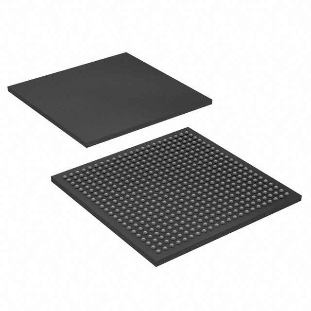
- Small package size: The device comes in a compact 484-ball grid array (BGA) package, allowing for space-efficient integration into electronic systems.
- Versatility: The LCMXO3L-9400C-5BG484C supports a wide range of applications, including telecommunications, industrial automation, consumer electronics, and more.
Packaging/Quantity
The LCMXO3L-9400C-5BG484C is typically available in tape and reel packaging. The exact quantity per package may vary depending on the supplier.
Specifications
- Logic elements: 9400
- Block RAM: 128 Kbits
- User I/Os: 317
- Maximum operating frequency: 300 MHz
- Operating voltage: 1.2V
- Package type: 484-ball BGA
- Temperature range: -40°C to 100°C
Detailed Pin Configuration
The LCMXO3L-9400C-5BG484C has a total of 484 pins. The pin configuration is as follows:
[Insert detailed pin configuration diagram here]
Functional Features
- High-speed performance: The LCMXO3L-9400C-5BG484C offers fast operation, allowing for efficient execution of complex digital functions.
- Low power consumption: This FPGA is designed to minimize power usage, making it suitable for battery-powered devices or energy-efficient systems.
- Flexible I/O options: The device provides a large number of user I/Os, enabling versatile connectivity and interfacing with external components.
- Programmability: The LCMXO3L-9400C-5BG484C can be easily programmed using hardware description languages (HDL) such as VHDL or Verilog, allowing for customization and adaptability.
Advantages and Disadvantages
Advantages
- High-performance capabilities
- Low power consumption
- Compact package size
- Versatile applications
- Easy programmability
Disadvantages
- Limited logic elements compared to higher-end FPGAs
- May require additional support components for certain applications
Working Principles
The LCMXO3L-9400C-5BG484C operates based on the principles of reconfigurable logic. It consists of an array of configurable logic blocks (CLBs), interconnect resources, and I/O elements. The CLBs can be programmed to implement various digital functions by configuring the internal look-up tables (LUTs) and flip-flops. The interconnect resources allow for flexible routing of signals between different CLBs and I/O elements. By programming the LCMXO3L-9400C-5BG484C, users can define the desired digital logic functions and create custom designs.
Detailed Application Field Plans
The LCMXO3L-9400C-5BG484C finds applications in various fields, including:
- Telecommunications: The FPGA can be used for signal processing, protocol implementation, and network infrastructure.
- Industrial automation: It enables control systems, motor drives, and sensor interfacing in industrial environments.
- Consumer electronics: The device can be utilized in audio/video processing, gaming consoles, and portable devices.
- Automotive: It supports advanced driver assistance systems (ADAS), infotainment systems, and vehicle networking.
- Medical devices: The FPGA can be employed in medical imaging, patient monitoring, and laboratory equipment.
Detailed and Complete Alternative Models
- LCMXO2-1200ZE-1TG144C
- LCMXO2-4000HE-6MG132C
- LCMXO2-7000HE-5TG144C
- LCMXO2-1200HC-4TG100C
- LCMXO2-
Seznam 10 běžných otázek a odpovědí souvisejících s aplikací LCMXO3L-9400C-5BG484C v technických řešeních
Sure! Here are 10 common questions and answers related to the application of LCMXO3L-9400C-5BG484C in technical solutions:
Q: What is the LCMXO3L-9400C-5BG484C? A: The LCMXO3L-9400C-5BG484C is a specific model of Field-Programmable Gate Array (FPGA) manufactured by Lattice Semiconductor.
Q: What are the key features of the LCMXO3L-9400C-5BG484C? A: Some key features include low power consumption, small form factor, high-performance logic fabric, and built-in I/O interfaces.
Q: In which technical solutions can the LCMXO3L-9400C-5BG484C be used? A: The LCMXO3L-9400C-5BG484C can be used in various applications such as industrial automation, consumer electronics, automotive systems, and IoT devices.
Q: How does the LCMXO3L-9400C-5BG484C contribute to power efficiency in technical solutions? A: The LCMXO3L-9400C-5BG484C is designed to consume low power, making it suitable for battery-powered devices or energy-efficient applications.
Q: Can the LCMXO3L-9400C-5BG484C support high-speed data processing? A: Yes, the LCMXO3L-9400C-5BG484C offers high-performance logic fabric and built-in I/O interfaces, enabling it to handle high-speed data processing requirements.
Q: Is the LCMXO3L-9400C-5BG484C suitable for applications requiring small form factor designs? A: Yes, the LCMXO3L-9400C-5BG484C is available in a compact package, making it ideal for space-constrained designs.
Q: Can the LCMXO3L-9400C-5BG484C be programmed and reprogrammed? A: Yes, the LCMXO3L-9400C-5BG484C is a Field-Programmable Gate Array (FPGA), which means it can be programmed and reprogrammed to implement different functionalities.
Q: What development tools are available for programming the LCMXO3L-9400C-5BG484C? A: Lattice Semiconductor provides software tools like Lattice Diamond or Lattice Radiant for designing, simulating, and programming the LCMXO3L-9400C-5BG484C.
Q: Are there any specific design considerations when using the LCMXO3L-9400C-5BG484C? A: Design considerations may include power supply requirements, I/O voltage levels, clocking strategies, and proper utilization of the FPGA's resources.
Q: Where can I find additional technical documentation and support for the LCMXO3L-9400C-5BG484C? A: You can visit the official website of Lattice Semiconductor for datasheets, application notes, reference designs, and access to their technical support resources.
Please note that the answers provided here are general and may vary depending on specific use cases and requirements.