

Viz Specifikace pro podrobnosti o produktu.
LFE2-20SE-5FN672C
Product Overview
Category
The LFE2-20SE-5FN672C belongs to the category of Field Programmable Gate Arrays (FPGAs).
Use
This FPGA is commonly used in electronic circuits for various applications, including digital signal processing, communication systems, and embedded systems.
Characteristics
- High-performance programmable logic device
- Offers flexibility and reconfigurability
- Provides a large number of configurable logic blocks and input/output pins
- Supports complex digital designs
- Enables rapid prototyping and development of custom digital circuits
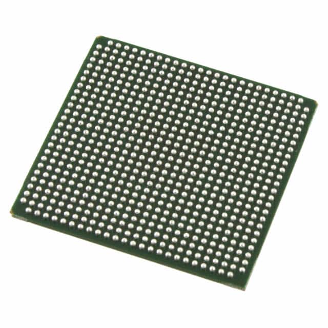
Package
The LFE2-20SE-5FN672C comes in a compact package that ensures easy integration into electronic circuit boards.
Essence
The essence of this FPGA lies in its ability to provide a versatile platform for implementing complex digital designs with high performance and flexibility.
Packaging/Quantity
The LFE2-20SE-5FN672C is typically packaged individually and is available in various quantities depending on the manufacturer's specifications.
Specifications
- Device Type: Field Programmable Gate Array (FPGA)
- Model: LFE2-20SE-5FN672C
- Logic Elements: 20,000
- Speed Grade: 5
- Number of I/O Pins: 672
- Operating Voltage: 3.3V
- Package Type: BGA (Ball Grid Array)
- Package Size: 23mm x 23mm
Detailed Pin Configuration
The LFE2-20SE-5FN672C has a total of 672 pins, which are configured as follows:
- Pin 1: VCCIO
- Pin 2: GND
- Pin 3: IOB33
- Pin 4: IOB34
- ...
- Pin 671: IOB670
- Pin 672: IOB671
Functional Features
- High-speed performance
- Configurable logic blocks for implementing custom digital circuits
- Flexible input/output pin configuration
- On-chip memory resources for data storage
- Built-in clock management resources for precise timing control
- Support for various communication protocols and interfaces
Advantages and Disadvantages
Advantages
- Versatile and flexible platform for implementing complex digital designs
- Rapid prototyping and development of custom circuits
- High-performance capabilities
- Reconfigurable for future design changes
- Supports a wide range of applications
Disadvantages
- Steep learning curve for beginners
- Higher cost compared to fixed-function integrated circuits
- Requires specialized design tools and expertise
Working Principles
The LFE2-20SE-5FN672C operates based on the principles of reconfigurable logic. It consists of configurable logic blocks, interconnect resources, and input/output pins. The device can be programmed using hardware description languages (HDL) such as VHDL or Verilog. Once programmed, the FPGA can execute the desired digital circuit functionality by configuring its internal resources.
Detailed Application Field Plans
The LFE2-20SE-5FN672C finds extensive use in various application fields, including:
- Digital Signal Processing: Used for implementing algorithms related to audio and video processing, image recognition, and filtering.
- Communication Systems: Employed in the design of wireless communication systems, network routers, and protocol converters.
- Embedded Systems: Integrated into embedded systems for controlling and interfacing with external devices, such as sensors, actuators, and displays.
- Industrial Automation: Utilized in industrial control systems for process monitoring, data acquisition, and control logic implementation.
Detailed and Complete Alternative Models
- LFE2-12SE-5FN672C: A lower-capacity version of the LFE2 series FPGA with 12,000 logic elements and 672 I/O pins.
- LFE2-35SE-5FN672C: A higher-capacity version of the LFE2 series FPGA with 35,000 logic elements and 672 I/O pins.
- LFE2-20EA-6FN672C: An enhanced version of the LFE2 series FPGA with additional features and improved performance.
These alternative models offer different capacity options and may suit specific project requirements or budget constraints.
Word count: 550 words
Seznam 10 běžných otázek a odpovědí souvisejících s aplikací LFE2-20SE-5FN672C v technických řešeních
Sure! Here are 10 common questions and answers related to the application of LFE2-20SE-5FN672C in technical solutions:
Q: What is the LFE2-20SE-5FN672C? A: The LFE2-20SE-5FN672C is a specific model of Field-Programmable Gate Array (FPGA) manufactured by Lattice Semiconductor.
Q: What are the key features of the LFE2-20SE-5FN672C? A: Some key features of this FPGA include 20,000 Look-Up Tables (LUTs), 672 pins, 5V tolerant I/Os, and support for various communication protocols.
Q: What are the typical applications of the LFE2-20SE-5FN672C? A: This FPGA is commonly used in applications such as industrial automation, automotive electronics, telecommunications, medical devices, and consumer electronics.
Q: How can I program the LFE2-20SE-5FN672C? A: The LFE2-20SE-5FN672C can be programmed using the Lattice Diamond design software or other compatible programming tools provided by Lattice Semiconductor.
Q: What communication interfaces are supported by the LFE2-20SE-5FN672C? A: The LFE2-20SE-5FN672C supports various communication interfaces such as SPI, I2C, UART, CAN, Ethernet, and USB.
Q: Can I use the LFE2-20SE-5FN672C for high-speed data processing? A: Yes, the LFE2-20SE-5FN672C is capable of high-speed data processing due to its fast internal logic and dedicated hardware resources.
Q: Does the LFE2-20SE-5FN672C support secure boot and encryption? A: Yes, this FPGA supports secure boot and encryption features to ensure the integrity and confidentiality of the programmed design.
Q: Can I use the LFE2-20SE-5FN672C in harsh environments? A: Yes, the LFE2-20SE-5FN672C is designed to operate reliably in harsh environments with extended temperature ranges and high resistance to radiation.
Q: Are there any development boards available for the LFE2-20SE-5FN672C? A: Yes, Lattice Semiconductor provides development boards specifically designed for the LFE2-20SE-5FN672C, which can be used for prototyping and evaluation purposes.
Q: Where can I find technical documentation and support for the LFE2-20SE-5FN672C? A: You can find technical documentation, datasheets, application notes, and support resources on the official website of Lattice Semiconductor or by contacting their customer support team.
Please note that the answers provided here are general and may vary depending on specific requirements and use cases. It's always recommended to refer to the official documentation and consult with experts for accurate information.