

Viz Specifikace pro podrobnosti o produktu.
LFE2-70E-6FN900C
Product Overview
Category
The LFE2-70E-6FN900C belongs to the category of Field Programmable Gate Arrays (FPGAs).
Use
This FPGA is commonly used in electronic circuits for various applications such as digital signal processing, telecommunications, and embedded systems.
Characteristics
- High-performance programmable logic device
- Offers flexibility and reconfigurability
- Provides a large number of configurable logic blocks and input/output pins
- Supports complex digital designs
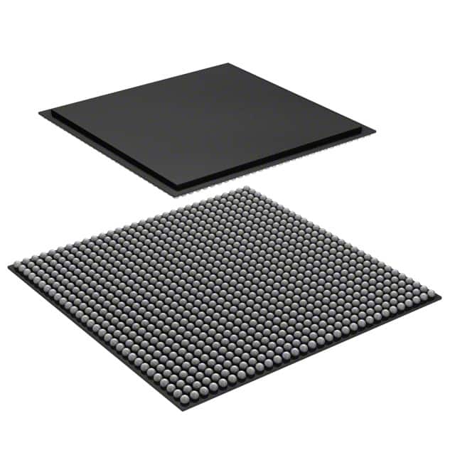
Package
The LFE2-70E-6FN900C comes in a compact and durable package suitable for integration into electronic systems.
Essence
The essence of this FPGA lies in its ability to be programmed and reprogrammed to perform specific functions, making it highly versatile and adaptable.
Packaging/Quantity
The LFE2-70E-6FN900C is typically packaged individually and is available in varying quantities depending on the manufacturer or supplier.
Specifications
- Model: LFE2-70E-6FN900C
- Logic Elements: 70,000
- Number of I/O Pins: 900
- Operating Voltage: 1.2V
- Maximum Frequency: 500 MHz
- Configuration Memory: 6 Mbits
- Package Type: FN900C
Detailed Pin Configuration
The LFE2-70E-6FN900C has a total of 900 pins, each serving a specific purpose in the circuit design. The detailed pin configuration can be found in the product datasheet provided by the manufacturer.
Functional Features
- High-speed data processing capabilities
- Configurable I/O standards
- Embedded memory blocks for efficient storage
- Dedicated clock management resources
- Support for various communication protocols
- Built-in security features for protecting intellectual property
Advantages and Disadvantages
Advantages
- Flexibility and reconfigurability allow for rapid prototyping and design iterations
- High-performance capabilities enable complex digital designs
- Wide range of I/O pins provide connectivity options
- Embedded memory blocks enhance data storage efficiency
Disadvantages
- Steeper learning curve compared to traditional fixed-function integrated circuits
- Higher power consumption compared to application-specific integrated circuits (ASICs)
- Limited scalability beyond a certain complexity level
Working Principles
The LFE2-70E-6FN900C operates based on the principles of programmable logic. It consists of configurable logic blocks, input/output pins, and interconnect resources. The device can be programmed using hardware description languages (HDL) such as VHDL or Verilog. Once programmed, the FPGA executes the desired logic functions by routing signals through its internal resources.
Detailed Application Field Plans
The LFE2-70E-6FN900C finds applications in various fields, including but not limited to: - Digital signal processing - Telecommunications - Embedded systems - Industrial automation - Aerospace and defense - Medical devices
Detailed and Complete Alternative Models
- LFE2-35E-5FN672C
- LFE2-100E-7FN484C
- LFE3-150EA-8FN672C
- LFE5U-45F-8BG381C
These alternative models offer different specifications and features, catering to diverse project requirements.
In conclusion, the LFE2-70E-6FN900C is a high-performance FPGA that provides flexibility, reconfigurability, and a wide range of applications. Its advanced features and characteristics make it suitable for various industries, enabling designers to implement complex digital designs efficiently.
Seznam 10 běžných otázek a odpovědí souvisejících s aplikací LFE2-70E-6FN900C v technických řešeních
Sure! Here are 10 common questions and answers related to the application of LFE2-70E-6FN900C in technical solutions:
Q: What is the LFE2-70E-6FN900C? A: The LFE2-70E-6FN900C is a field-programmable gate array (FPGA) manufactured by Lattice Semiconductor.
Q: What are the key features of the LFE2-70E-6FN900C? A: The key features of the LFE2-70E-6FN900C include 70,000 logic elements, 900 MHz maximum operating frequency, and low power consumption.
Q: What are some typical applications of the LFE2-70E-6FN900C? A: The LFE2-70E-6FN900C is commonly used in applications such as telecommunications, industrial automation, automotive electronics, and medical devices.
Q: How can I program the LFE2-70E-6FN900C? A: The LFE2-70E-6FN900C can be programmed using various design software tools provided by Lattice Semiconductor, such as Lattice Diamond or Lattice Radiant.
Q: What is the maximum operating frequency of the LFE2-70E-6FN900C? A: The LFE2-70E-6FN900C has a maximum operating frequency of 900 MHz, making it suitable for high-performance applications.
Q: Does the LFE2-70E-6FN900C support different I/O standards? A: Yes, the LFE2-70E-6FN900C supports various I/O standards, including LVCMOS, LVTTL, LVDS, and SSTL.
Q: Can I use the LFE2-70E-6FN900C in a low-power application? A: Yes, the LFE2-70E-6FN900C is designed to be power-efficient, making it suitable for low-power applications where energy consumption is a concern.
Q: What are the available package options for the LFE2-70E-6FN900C? A: The LFE2-70E-6FN900C is available in a 900-ball fine pitch ball grid array (FBGA) package.
Q: Does the LFE2-70E-6FN900C have built-in security features? A: Yes, the LFE2-70E-6FN900C offers built-in security features such as bitstream encryption and authentication to protect against unauthorized access or tampering.
Q: Where can I find more information about the LFE2-70E-6FN900C? A: You can find more detailed information about the LFE2-70E-6FN900C, including datasheets, application notes, and reference designs, on the official website of Lattice Semiconductor or by contacting their technical support team.