

Viz Specifikace pro podrobnosti o produktu.
LFE2M100SE-6FN1152C
Product Overview
Category
The LFE2M100SE-6FN1152C belongs to the category of Field Programmable Gate Arrays (FPGAs).
Use
This FPGA is primarily used for digital logic applications, such as in embedded systems, telecommunications, and high-performance computing.
Characteristics
- High-speed performance
- Configurable logic blocks
- On-chip memory
- Flexible I/O options
- Low power consumption
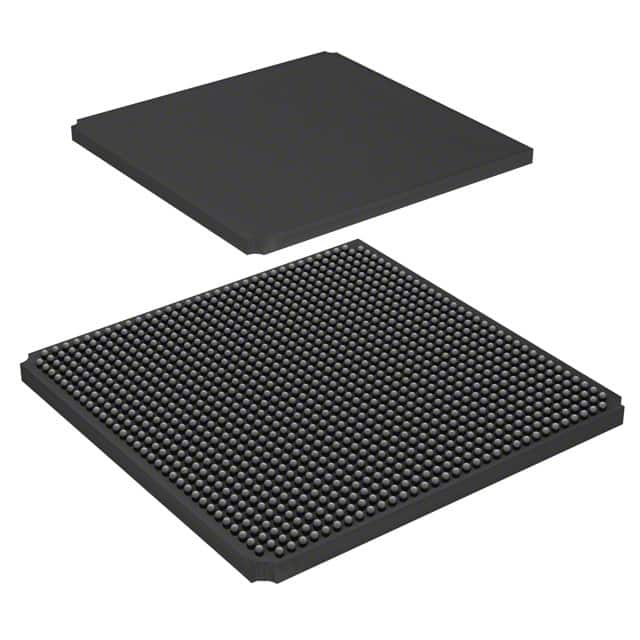
Package
The LFE2M100SE-6FN1152C comes in a compact package that ensures easy integration into various electronic systems. It is designed to be surface-mounted on printed circuit boards (PCBs).
Essence
The essence of the LFE2M100SE-6FN1152C lies in its ability to provide reconfigurable hardware that can be customized to perform specific tasks efficiently.
Packaging/Quantity
The LFE2M100SE-6FN1152C is typically packaged in trays or reels, depending on the manufacturer's specifications. The quantity per package may vary, but it is commonly available in quantities suitable for both prototyping and production purposes.
Specifications
- FPGA Family: Lattice ECP2M
- Device Type: LFE2M100SE
- Logic Cells: 100,000
- Speed Grade: -6
- Number of I/Os: 1,152
- Operating Voltage: 1.2V
- Package Type: FN1152C
Detailed Pin Configuration
The LFE2M100SE-6FN1152C has a comprehensive pin configuration that allows for versatile connectivity. Please refer to the datasheet provided by the manufacturer for the detailed pinout information.
Functional Features
- High-speed data processing capabilities
- Configurable logic blocks for flexible design implementation
- On-chip memory for efficient data storage and retrieval
- Multiple I/O options to interface with external devices
- Low power consumption for energy-efficient operation
Advantages and Disadvantages
Advantages
- Versatile and customizable hardware solution
- High-performance capabilities
- Efficient use of resources
- Wide range of application possibilities
Disadvantages
- Steep learning curve for beginners
- Requires specialized design tools and knowledge
- Relatively higher cost compared to other solutions for simpler applications
Working Principles
The LFE2M100SE-6FN1152C operates based on the principles of reconfigurable logic. It consists of configurable logic blocks interconnected through programmable routing resources. The device can be programmed to implement various digital logic functions, allowing for flexible and efficient system designs.
Detailed Application Field Plans
The LFE2M100SE-6FN1152C finds applications in a wide range of fields, including but not limited to: - Embedded systems - Telecommunications infrastructure - High-performance computing - Industrial automation - Aerospace and defense
Detailed and Complete Alternative Models
- LFE2M200SE-6FN1152C: Similar to LFE2M100SE-6FN1152C but with double the logic cells for more complex designs.
- LFE2M50SE-6FN1152C: A lower-cost alternative with fewer logic cells suitable for simpler applications.
- LFE2M150SE-6FN1152C: An enhanced version with additional features and improved performance.
Please note that the above list is not exhaustive, and there may be other alternative models available from different manufacturers.
Word count: 440 words
Seznam 10 běžných otázek a odpovědí souvisejících s aplikací LFE2M100SE-6FN1152C v technických řešeních
Sure! Here are 10 common questions and answers related to the application of LFE2M100SE-6FN1152C in technical solutions:
Q: What is the LFE2M100SE-6FN1152C? A: The LFE2M100SE-6FN1152C is a specific model of Field-Programmable Gate Array (FPGA) manufactured by Lattice Semiconductor.
Q: What are the key features of the LFE2M100SE-6FN1152C? A: Some key features of this FPGA include 100,000 logic elements, 1.15 million bits of embedded memory, 6-input look-up tables, and support for various I/O standards.
Q: What are the typical applications of the LFE2M100SE-6FN1152C? A: This FPGA is commonly used in applications such as industrial automation, automotive electronics, telecommunications, medical devices, and high-performance computing.
Q: How can I program the LFE2M100SE-6FN1152C? A: You can program this FPGA using the Lattice Diamond design software or other compatible programming tools provided by Lattice Semiconductor.
Q: What are the power requirements for the LFE2M100SE-6FN1152C? A: The typical operating voltage range for this FPGA is 1.14V to 1.26V, and it requires a stable power supply with appropriate current capabilities.
Q: Can I interface the LFE2M100SE-6FN1152C with other components or devices? A: Yes, this FPGA supports various communication interfaces such as SPI, I2C, UART, and LVDS, allowing you to interface it with other components or devices in your system.
Q: Does the LFE2M100SE-6FN1152C support security features? A: Yes, this FPGA provides built-in security features like bitstream encryption and authentication to protect your intellectual property and prevent unauthorized access.
Q: What kind of development tools are available for the LFE2M100SE-6FN1152C? A: Lattice Semiconductor provides a comprehensive suite of development tools, including design software, simulation tools, and debugging utilities, to aid in the development process.
Q: Can I use the LFE2M100SE-6FN1152C for real-time signal processing applications? A: Yes, this FPGA is capable of handling real-time signal processing tasks due to its high logic capacity, embedded memory, and support for various DSP functions.
Q: Where can I find more technical information about the LFE2M100SE-6FN1152C? A: You can refer to the datasheet, user manual, application notes, and other technical documentation provided by Lattice Semiconductor on their official website for detailed information about this FPGA.
Please note that the specific details and answers may vary depending on the manufacturer's specifications and documentation.