

Viz Specifikace pro podrobnosti o produktu.
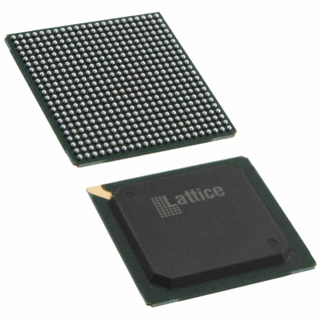
LFE2M35SE-5F484I
Product Overview
Category
The LFE2M35SE-5F484I belongs to the category of Field Programmable Gate Arrays (FPGAs).
Use
This FPGA is commonly used in various electronic applications that require programmable logic devices. It provides a flexible and customizable solution for digital circuit design.
Characteristics
- High-performance FPGA with advanced features
- Offers reconfigurable logic elements and embedded memory blocks
- Supports various I/O standards and interfaces
- Provides efficient power management capabilities
- Enables rapid prototyping and development of complex digital systems
Package
The LFE2M35SE-5F484I comes in a compact and durable package, designed to ensure reliable operation even in demanding environments.
Essence
The essence of this FPGA lies in its ability to provide a versatile platform for implementing complex digital designs. Its programmable nature allows for customization and adaptation to specific application requirements.
Packaging/Quantity
The LFE2M35SE-5F484I is typically packaged individually and is available in various quantities depending on the customer's needs.
Specifications
- Logic Elements: 35,000
- Embedded Memory Blocks: 1,080 Kbits
- Maximum User I/Os: 315
- Clock Management Tiles: 8
- Maximum Operating Frequency: 400 MHz
- Supply Voltage: 1.2V
- Package Type: 484-pin FineLine BGA
Detailed Pin Configuration
The LFE2M35SE-5F484I has a total of 484 pins, each serving a specific purpose in the FPGA's functionality. The pin configuration includes dedicated inputs and outputs for various signals, power supply pins, and configuration interface pins.
For a detailed pin configuration diagram, please refer to the manufacturer's datasheet.
Functional Features
- Reconfigurable logic elements allow for flexible implementation of digital circuits.
- Embedded memory blocks provide additional storage capacity for data processing.
- Clock management tiles enable precise control and distribution of clock signals.
- Support for various I/O standards and interfaces facilitates seamless integration with external devices.
- Efficient power management capabilities optimize power consumption.
Advantages and Disadvantages
Advantages
- Versatile and customizable solution for digital circuit design.
- Rapid prototyping and development of complex systems.
- High-performance FPGA with advanced features.
- Efficient power management capabilities.
Disadvantages
- Steep learning curve for beginners due to the complexity of FPGA programming.
- Limited availability of alternative models with similar specifications.
Working Principles
The LFE2M35SE-5F484I operates based on the principles of reconfigurable logic. It consists of a matrix of programmable logic elements interconnected through configurable routing resources. These logic elements can be programmed to implement various digital functions, allowing for the creation of complex circuits.
The FPGA's configuration is stored in non-volatile memory and can be modified as needed. During operation, input signals are processed by the logic elements according to the programmed configuration, producing the desired output signals.
Detailed Application Field Plans
The LFE2M35SE-5F484I finds applications in a wide range of fields, including:
- Communications: Used in wireless communication systems, network routers, and data transmission equipment.
- Industrial Automation: Employed in control systems, robotics, and process automation.
- Automotive: Integrated into automotive electronics for engine control, driver assistance systems, and infotainment.
- Aerospace: Utilized in avionics systems, satellite communication, and navigation equipment.
- Medical Devices: Incorporated into medical imaging systems, patient monitoring devices, and laboratory equipment.
Detailed and Complete Alternative Models
While the LFE2M35SE-5F484I offers advanced features and performance, alternative models with similar specifications include:
- LFE2M35SE-6F484I
- LFE2M35SE-7F484I
- LFE2M35SE-8F484I
These alternative models provide comparable functionality and can be considered based on specific project requirements.
In conclusion, the LFE2M35SE-5F484I is a high-performance FPGA that offers flexibility, advanced features, and efficient power management capabilities. Its versatile nature makes it suitable for various applications in different fields. While it may have a steep learning curve for beginners and limited availability of alternative models, its advantages outweigh the disadvantages, making it a valuable tool for digital circuit design and development.
Seznam 10 běžných otázek a odpovědí souvisejících s aplikací LFE2M35SE-5F484I v technických řešeních
Sure! Here are 10 common questions and answers related to the application of LFE2M35SE-5F484I in technical solutions:
Q: What is LFE2M35SE-5F484I? A: LFE2M35SE-5F484I is a specific model of Field-Programmable Gate Array (FPGA) manufactured by Lattice Semiconductor.
Q: What are the key features of LFE2M35SE-5F484I? A: Some key features of LFE2M35SE-5F484I include 35,000 Look-Up Tables (LUTs), 1,080 Kbits of embedded memory, 184 user I/O pins, and support for various communication protocols.
Q: What are the typical applications of LFE2M35SE-5F484I? A: LFE2M35SE-5F484I is commonly used in applications such as industrial automation, automotive electronics, telecommunications, medical devices, and consumer electronics.
Q: How can LFE2M35SE-5F484I be programmed? A: LFE2M35SE-5F484I can be programmed using hardware description languages (HDLs) like VHDL or Verilog, which are then synthesized and implemented using appropriate software tools provided by Lattice Semiconductor.
Q: Can LFE2M35SE-5F484I be reprogrammed after initial programming? A: Yes, LFE2M35SE-5F484I is a reprogrammable FPGA, allowing for multiple iterations of design changes and updates.
Q: What are the power requirements for LFE2M35SE-5F484I? A: The power requirements for LFE2M35SE-5F484I typically include a supply voltage of 3.3V and various current specifications depending on the application.
Q: Does LFE2M35SE-5F484I support different communication protocols? A: Yes, LFE2M35SE-5F484I supports various communication protocols such as SPI, I2C, UART, and Ethernet, making it versatile for interfacing with other devices.
Q: Can LFE2M35SE-5F484I interface with external memory devices? A: Yes, LFE2M35SE-5F484I has embedded memory blocks and can also interface with external memory devices like DDR SDRAM or Flash memory.
Q: What development tools are available for programming LFE2M35SE-5F484I? A: Lattice Semiconductor provides software tools like Lattice Diamond or Lattice Radiant, which offer design entry, synthesis, simulation, and programming capabilities for LFE2M35SE-5F484I.
Q: Are there any reference designs or application notes available for LFE2M35SE-5F484I? A: Yes, Lattice Semiconductor provides a range of reference designs, application notes, and technical documentation to assist users in implementing LFE2M35SE-5F484I in their specific technical solutions.
Please note that the answers provided here are general and may vary based on specific requirements and implementation details.