

Viz Specifikace pro podrobnosti o produktu.
LFE2M50E-5FN484I
Product Overview
Category
The LFE2M50E-5FN484I belongs to the category of Field Programmable Gate Arrays (FPGAs).
Use
FPGAs are integrated circuits that can be programmed and reprogrammed to perform various digital functions. The LFE2M50E-5FN484I is specifically designed for applications requiring high-performance and low-power consumption.
Characteristics
- High-performance FPGA with low power consumption
- Flexible and reprogrammable design
- Suitable for a wide range of applications
- Compact package size
- Robust and reliable performance
Package
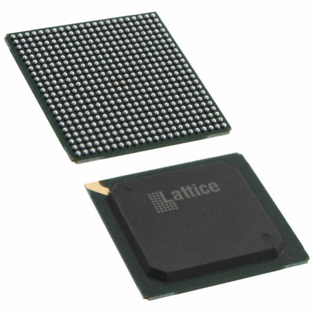
The LFE2M50E-5FN484I comes in a 484-pin FineLine BGA (Ball Grid Array) package.
Essence
The essence of the LFE2M50E-5FN484I lies in its ability to provide a versatile and efficient solution for digital circuit implementation. It offers a balance between performance, power consumption, and flexibility.
Packaging/Quantity
The LFE2M50E-5FN484I is typically packaged individually and is available in various quantities depending on the manufacturer's specifications.
Specifications
- FPGA Family: Lattice ECP2M
- Logic Elements: 50,000
- Number of I/O Pins: 484
- Operating Voltage: 1.2V
- Maximum Frequency: Up to 400 MHz
- Embedded Memory: Up to 4.8 Mb
- DSP Slices: Up to 96
- Configuration Memory: On-chip Flash
Detailed Pin Configuration
The LFE2M50E-5FN484I has a total of 484 pins, each serving a specific purpose in the overall functionality of the FPGA. A detailed pin configuration diagram can be found in the product datasheet provided by the manufacturer.
Functional Features
- High-performance digital circuit implementation
- Low power consumption for energy-efficient applications
- Flexible and reprogrammable design allows for easy customization
- On-chip memory for efficient data storage and retrieval
- DSP slices for implementing complex mathematical operations
- Support for various communication protocols and interfaces
Advantages and Disadvantages
Advantages
- High-performance capabilities suitable for demanding applications
- Low power consumption for energy-efficient designs
- Flexibility to adapt to changing requirements
- Compact package size for space-constrained applications
- On-chip memory eliminates the need for external memory components
Disadvantages
- Limited logic elements compared to larger FPGAs
- Higher cost compared to simpler programmable logic devices
- Steeper learning curve for programming and utilizing the FPGA's full potential
Working Principles
The LFE2M50E-5FN484I operates based on the principles of configurable logic. It consists of a matrix of programmable logic elements interconnected through configurable routing resources. The user can program the FPGA using hardware description languages (HDLs) or graphical tools to define the desired functionality. Once programmed, the FPGA executes the specified digital circuit operations.
Detailed Application Field Plans
The LFE2M50E-5FN484I finds applications in various fields, including but not limited to: - Telecommunications - Industrial automation - Automotive electronics - Medical devices - Aerospace and defense systems - Consumer electronics
In telecommunications, the FPGA can be used for signal processing, protocol conversion, and network optimization. In industrial automation, it enables control and monitoring of complex machinery. Automotive electronics benefit from its ability to handle advanced driver assistance systems (ADAS) and infotainment functionalities. Medical devices utilize the FPGA for image processing, diagnostics, and patient monitoring. Aerospace and defense systems rely on its high-performance capabilities for radar processing, communication systems, and encryption. Lastly, consumer electronics applications include video and audio processing, gaming, and data storage.
Detailed and Complete Alternative Models
- Xilinx Virtex-7 XC7VX485T
- Intel Cyclone V EP5CE115F23I7N
- Microsemi SmartFusion2 M2S150T-1FGG484I
- Actel ProASIC3 A3P1000-FG484I
- QuickLogic PolarPro 2 LP2-640
These alternative models offer similar functionalities and performance characteristics to the LFE2M50E-5FN484I, providing users with a range of options based on their specific requirements.
Word count: 570 words
Seznam 10 běžných otázek a odpovědí souvisejících s aplikací LFE2M50E-5FN484I v technických řešeních
Sure! Here are 10 common questions and answers related to the application of LFE2M50E-5FN484I in technical solutions:
1. What is the LFE2M50E-5FN484I? The LFE2M50E-5FN484I is a specific model of Field-Programmable Gate Array (FPGA) manufactured by Lattice Semiconductor.
2. What are the key features of the LFE2M50E-5FN484I? Some key features of this FPGA include 50,000 Look-Up Tables (LUTs), 1,152 Kbits of embedded memory, 184 user I/O pins, and support for various communication protocols.
3. What are the typical applications of the LFE2M50E-5FN484I? This FPGA is commonly used in applications such as industrial automation, telecommunications, automotive electronics, medical devices, and high-performance computing.
4. How can I program the LFE2M50E-5FN484I? You can program this FPGA using the Lattice Diamond design software or other compatible programming tools provided by Lattice Semiconductor.
5. What voltage levels does the LFE2M50E-5FN484I support? This FPGA supports both 3.3V and 1.2V voltage levels for different parts of its internal circuitry.
6. Can I interface the LFE2M50E-5FN484I with external devices? Yes, the FPGA provides 184 user I/O pins that can be used to interface with various external devices such as sensors, actuators, displays, and communication modules.
7. Does the LFE2M50E-5FN484I support any specific communication protocols? Yes, this FPGA supports popular communication protocols like SPI, I2C, UART, and Ethernet, making it suitable for a wide range of applications.
8. What is the power consumption of the LFE2M50E-5FN484I? The power consumption of this FPGA depends on the specific design and usage scenario. You can refer to the datasheet provided by Lattice Semiconductor for detailed power consumption information.
9. Can I use the LFE2M50E-5FN484I in safety-critical applications? Yes, this FPGA is designed to meet certain safety standards and can be used in safety-critical applications with proper design considerations and validation processes.
10. Are there any development boards available for the LFE2M50E-5FN484I? Yes, Lattice Semiconductor provides development boards specifically designed for this FPGA model, which can help in prototyping and testing your technical solutions.
Please note that the answers provided here are general and may vary depending on the specific requirements and implementation details of your technical solution.