

Viz Specifikace pro podrobnosti o produktu.
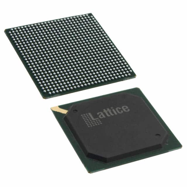
LFE2M50E-6FN672I
Product Overview
Category
The LFE2M50E-6FN672I belongs to the category of Field Programmable Gate Arrays (FPGAs).
Use
FPGAs are integrated circuits that can be programmed and reprogrammed to perform various digital functions. The LFE2M50E-6FN672I is specifically designed for applications requiring high-performance and low-power consumption.
Characteristics
- High performance: The LFE2M50E-6FN672I offers a combination of speed and flexibility, making it suitable for demanding applications.
- Low power consumption: This FPGA is designed to minimize power usage, making it energy-efficient.
- Programmability: The LFE2M50E-6FN672I can be easily programmed and reconfigured to adapt to different requirements.
- Versatility: It supports a wide range of digital functions and can be used in diverse applications.
Package and Quantity
The LFE2M50E-6FN672I comes in a 672-pin FineLine BGA package. The quantity may vary depending on the supplier or customer requirements.
Specifications
- Logic Elements: 50,000
- Embedded Memory: 1,728 Kbits
- Maximum User I/Os: 622
- Clock Management Tiles: 4
- DSP Blocks: 120
- Operating Voltage: 1.2V
- Operating Temperature Range: -40°C to 100°C
Detailed Pin Configuration
For detailed pin configuration information, please refer to the manufacturer's datasheet or technical documentation.
Functional Features
The LFE2M50E-6FN672I offers several functional features that enhance its performance and usability: - High-speed interfaces: It supports various high-speed interfaces such as DDR3, PCIe, and Ethernet, enabling seamless integration with other components. - Flexible I/O options: The FPGA provides a wide range of I/O options, allowing for versatile connectivity with external devices. - On-chip memory: The embedded memory blocks enable efficient data storage and retrieval, reducing the need for external memory components. - Clock management: The integrated clock management tiles offer precise control over clock signals, ensuring synchronization and timing accuracy.
Advantages and Disadvantages
Advantages: - High performance and flexibility - Low power consumption - Versatile I/O options - On-chip memory reduces external component requirements
Disadvantages: - Limited logic elements compared to higher-end FPGAs - Higher cost compared to some alternative solutions
Working Principles
FPGAs like the LFE2M50E-6FN672I consist of an array of configurable logic blocks interconnected through programmable routing resources. These logic blocks can be programmed to implement various digital functions by configuring the interconnections and functionality of the individual blocks. The configuration is typically done using Hardware Description Languages (HDL) or specialized design tools provided by the FPGA manufacturer.
Detailed Application Field Plans
The LFE2M50E-6FN672I finds applications in various fields, including but not limited to: - Communications: It can be used in networking equipment, wireless communication systems, and data transmission devices. - Industrial automation: The FPGA's high-performance capabilities make it suitable for industrial control systems, robotics, and process automation. - Medical devices: It can be utilized in medical imaging equipment, patient monitoring systems, and diagnostic devices. - Aerospace and defense: The FPGA's reliability and versatility make it ideal for aerospace applications, including avionics, radar systems, and satellite communication.
Detailed and Complete Alternative Models
- LFE2M35E-5FN484C: A lower-cost alternative with 35,000 logic elements and similar features.
- LFE3-150EA-8FN672C: A higher-end FPGA with 150,000 logic elements and enhanced performance capabilities.
- LCMXO2-1200ZE-1TG144I: A smaller-sized FPGA with 1,200 logic elements, suitable for low-power applications.
Please note that the above alternative models are provided as examples and there may be other alternatives available in the market.
In conclusion, the LFE2M50E-6FN672I is a high-performance FPGA with low power consumption. Its versatility, flexible I/O options, and on-chip memory make it suitable for various applications in fields such as communications, industrial automation, medical devices, and aerospace. While it has some limitations in terms of logic elements and cost, it offers significant advantages in terms of performance and programmability.
Seznam 10 běžných otázek a odpovědí souvisejících s aplikací LFE2M50E-6FN672I v technických řešeních
Sure! Here are 10 common questions and answers related to the application of LFE2M50E-6FN672I in technical solutions:
Q: What is the LFE2M50E-6FN672I? A: The LFE2M50E-6FN672I is a specific model of Field-Programmable Gate Array (FPGA) manufactured by Lattice Semiconductor.
Q: What are the key features of the LFE2M50E-6FN672I? A: The key features of this FPGA include 50,000 Look-Up Tables (LUTs), 672-pin FineLine BGA package, low power consumption, and high-speed performance.
Q: What are some typical applications for the LFE2M50E-6FN672I? A: This FPGA can be used in various applications such as industrial automation, telecommunications, automotive electronics, medical devices, and consumer electronics.
Q: How can I program the LFE2M50E-6FN672I? A: The LFE2M50E-6FN672I can be programmed using the Lattice Diamond design software or other compatible programming tools provided by Lattice Semiconductor.
Q: What is the maximum operating frequency of the LFE2M50E-6FN672I? A: The maximum operating frequency of this FPGA depends on the specific design and implementation, but it can typically reach frequencies of several hundred megahertz (MHz).
Q: Does the LFE2M50E-6FN672I support different I/O standards? A: Yes, this FPGA supports various I/O standards such as LVCMOS, LVTTL, LVDS, SSTL, and HSTL, allowing for compatibility with different interface requirements.
Q: Can I use the LFE2M50E-6FN672I in a high-reliability application? A: Yes, this FPGA is designed to meet the requirements of high-reliability applications and can operate in harsh environments with proper design considerations.
Q: What are the power supply requirements for the LFE2M50E-6FN672I? A: The LFE2M50E-6FN672I typically requires a single 3.3V power supply, but it also supports multiple power supply options for different voltage domains within the device.
Q: Are there any evaluation boards available for the LFE2M50E-6FN672I? A: Yes, Lattice Semiconductor provides evaluation boards and development kits specifically designed for the LFE2M50E-6FN672I, which can help in the prototyping and testing phase.
Q: Where can I find more technical documentation and support for the LFE2M50E-6FN672I? A: You can find more technical documentation, datasheets, application notes, and support resources on the official website of Lattice Semiconductor or by contacting their customer support team.
Please note that the answers provided here are general and may vary depending on specific requirements and implementation details.