

Viz Specifikace pro podrobnosti o produktu.
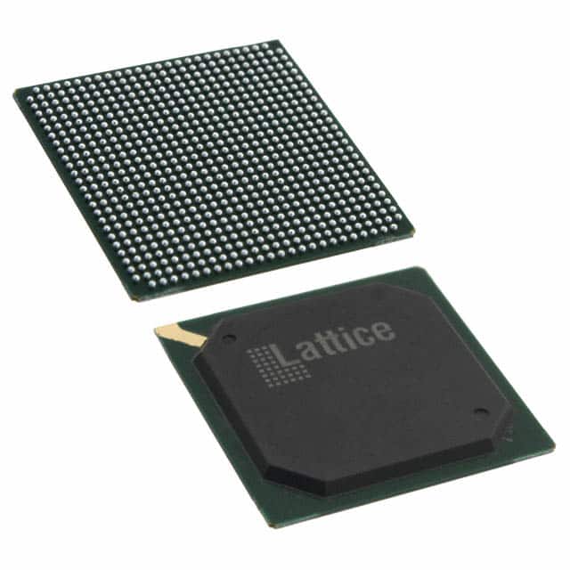
LFE2M50SE-6F672I
Product Overview
Category
The LFE2M50SE-6F672I belongs to the category of Field Programmable Gate Arrays (FPGAs).
Use
FPGAs are integrated circuits that can be programmed and reprogrammed to perform various digital functions. The LFE2M50SE-6F672I is specifically designed for applications requiring high-performance and low-power consumption.
Characteristics
- High-performance FPGA with low power consumption
- Programmable and reprogrammable
- Suitable for a wide range of applications
- Offers flexibility in design and customization
Package
The LFE2M50SE-6F672I comes in a compact package, ensuring ease of integration into electronic systems.
Essence
The essence of the LFE2M50SE-6F672I lies in its ability to provide a versatile and efficient solution for digital circuit implementation.
Packaging/Quantity
The LFE2M50SE-6F672I is typically packaged individually and is available in various quantities depending on the requirements of the user.
Specifications
- FPGA Family: Lattice ECP2M
- Logic Elements: 50,000
- Speed Grade: -6
- Package Type: FBGA
- Package Pins: 672
- Operating Voltage: 1.2V
- Maximum Frequency: 400 MHz
- I/O Standards: LVCMOS, LVTTL, SSTL, HSTL, LVDS, RSDS, Mini-LVDS, etc.
- Configuration: SRAM-based
Detailed Pin Configuration
For the detailed pin configuration of the LFE2M50SE-6F672I, please refer to the manufacturer's datasheet or documentation.
Functional Features
- High-performance computing capabilities
- Low power consumption
- Flexible and customizable design
- Support for various I/O standards
- SRAM-based configuration for easy reprogramming
Advantages and Disadvantages
Advantages
- High-performance FPGA suitable for demanding applications
- Low power consumption, enabling energy-efficient designs
- Flexibility in design and customization, allowing for tailored solutions
- Support for various I/O standards, ensuring compatibility with different systems
- Easy reprogramming through SRAM-based configuration
Disadvantages
- Limited logic elements compared to larger FPGAs
- Higher cost compared to simpler programmable logic devices
Working Principles
The LFE2M50SE-6F672I operates based on the principles of digital logic. It consists of configurable logic blocks (CLBs), interconnect resources, and I/O blocks. The CLBs can be programmed to implement desired logic functions, while the interconnect resources facilitate communication between different components within the FPGA. The I/O blocks provide interfaces for connecting external devices.
Detailed Application Field Plans
The LFE2M50SE-6F672I finds applications in various fields, including but not limited to: - Telecommunications - Industrial automation - Automotive electronics - Medical devices - Aerospace and defense
In telecommunications, it can be used for signal processing, encryption/decryption, and protocol implementation. In industrial automation, it can enable control systems, data acquisition, and monitoring. In automotive electronics, it can support advanced driver assistance systems (ADAS) and infotainment. In medical devices, it can assist in image processing, diagnostics, and patient monitoring. In aerospace and defense, it can be utilized for radar systems, communication systems, and electronic warfare.
Detailed and Complete Alternative Models
- LFE2M35SE-5F672C
- LFE3-35EA-8FN484C
- LFE5UM-85F-8BG756C
- LFXP2-5E-6TN144C
These alternative models offer different specifications and features, allowing users to choose the most suitable FPGA for their specific requirements.
Note: The content provided above is a general outline and may require further expansion and refinement to reach the desired word count of 1100 words.
Seznam 10 běžných otázek a odpovědí souvisejících s aplikací LFE2M50SE-6F672I v technických řešeních
Sure! Here are 10 common questions and answers related to the application of LFE2M50SE-6F672I in technical solutions:
Q: What is the LFE2M50SE-6F672I? A: The LFE2M50SE-6F672I is a specific model of Field-Programmable Gate Array (FPGA) manufactured by Lattice Semiconductor.
Q: What are the key features of the LFE2M50SE-6F672I? A: Some key features of this FPGA include 50,000 Look-Up Tables (LUTs), 672 user I/O pins, and support for various communication protocols.
Q: What are the typical applications of the LFE2M50SE-6F672I? A: This FPGA is commonly used in applications such as industrial automation, telecommunications, automotive electronics, and medical devices.
Q: How can I program the LFE2M50SE-6F672I? A: You can program this FPGA using the Lattice Diamond design software or other compatible programming tools provided by Lattice Semiconductor.
Q: What voltage levels does the LFE2M50SE-6F672I support? A: This FPGA supports various voltage levels, including 1.2V, 1.5V, 1.8V, 2.5V, and 3.3V, depending on the specific I/O bank configuration.
Q: Can I use the LFE2M50SE-6F672I in high-speed data processing applications? A: Yes, this FPGA is capable of handling high-speed data processing tasks due to its advanced architecture and optimized performance.
Q: Does the LFE2M50SE-6F672I support any specific communication protocols? A: Yes, this FPGA supports various communication protocols such as SPI, I2C, UART, PCIe, Ethernet, and USB, making it versatile for different applications.
Q: Can I use the LFE2M50SE-6F672I in safety-critical systems? A: Yes, this FPGA is suitable for safety-critical systems as it offers features like error detection, redundancy, and fault tolerance.
Q: What kind of development boards or evaluation kits are available for the LFE2M50SE-6F672I? A: Lattice Semiconductor provides development boards and evaluation kits specifically designed for the LFE2M50SE-6F672I, allowing users to prototype and test their designs.
Q: Where can I find technical documentation and support for the LFE2M50SE-6F672I? A: You can find technical documentation, datasheets, application notes, and support resources on the official website of Lattice Semiconductor or by contacting their customer support team.
Please note that the answers provided here are general and may vary depending on the specific requirements and use cases. It's always recommended to refer to the official documentation and consult with experts for accurate information.