

Viz Specifikace pro podrobnosti o produktu.
LFE2M50SE-6FN484I
Product Overview
Category
The LFE2M50SE-6FN484I belongs to the category of Field Programmable Gate Arrays (FPGAs).
Use
FPGAs are integrated circuits that can be programmed and reprogrammed to perform various digital functions. The LFE2M50SE-6FN484I is specifically designed for applications requiring high-performance and low-power consumption.
Characteristics
- High-performance FPGA with low power consumption
- Flexible and reprogrammable design
- Suitable for a wide range of applications
- Compact package for easy integration
Package
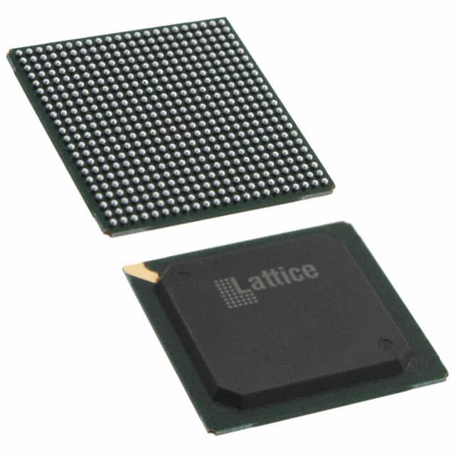
The LFE2M50SE-6FN484I comes in a 484-pin FineLine BGA (Ball Grid Array) package.
Essence
The essence of the LFE2M50SE-6FN484I lies in its ability to provide a customizable and efficient solution for digital circuit implementation.
Packaging/Quantity
The LFE2M50SE-6FN484I is typically sold individually or in small quantities, depending on the supplier.
Specifications
- FPGA Family: LatticeECP2M
- Logic Elements: 50,000
- Speed Grade: -6
- Package Type: FN484
- I/O Pins: 484
- Operating Voltage: 1.2V
- Maximum Frequency: 400 MHz
- Embedded Memory: Up to 4.8 Mbits
- DSP Slices: 96
- PLLs: 4
Detailed Pin Configuration
The LFE2M50SE-6FN484I has 484 pins, each serving a specific purpose in the overall functionality of the FPGA. A detailed pin configuration diagram can be found in the product datasheet.
Functional Features
- High-speed performance with low power consumption
- Configurable logic elements for custom digital circuit implementation
- Embedded memory blocks for data storage
- Digital Signal Processing (DSP) slices for efficient signal processing
- Phase-Locked Loops (PLLs) for clock management and synchronization
Advantages and Disadvantages
Advantages
- High-performance FPGA suitable for demanding applications
- Low power consumption for energy-efficient designs
- Flexible and reprogrammable architecture allows for customization
- Compact package enables easy integration into various systems
Disadvantages
- Limited availability of alternative models with similar specifications
- Steep learning curve for programming and utilizing the full potential of the FPGA
Working Principles
The LFE2M50SE-6FN484I operates based on the principles of configurable logic elements, which can be programmed to perform specific digital functions. These logic elements are interconnected through programmable interconnects, allowing for the creation of complex digital circuits. The FPGA is configured using a Hardware Description Language (HDL) such as VHDL or Verilog.
Detailed Application Field Plans
The LFE2M50SE-6FN484I finds applications in various fields, including:
- Telecommunications: Used in base stations, routers, and network switches for high-speed data processing.
- Industrial Automation: Employed in control systems, robotics, and machine vision applications for real-time processing and control.
- Automotive: Integrated into advanced driver assistance systems (ADAS), infotainment systems, and engine control units (ECUs) for enhanced functionality.
- Aerospace and Defense: Utilized in radar systems, avionics, and communication equipment for reliable and high-performance operation.
- Medical Devices: Incorporated into medical imaging systems, patient monitoring devices, and laboratory equipment for data processing and analysis.
Detailed and Complete Alternative Models
While the LFE2M50SE-6FN484I offers unique features and specifications, alternative models with similar capabilities include:
- Xilinx Spartan-6 FPGA
- Altera Cyclone IV FPGA
- Microsemi SmartFusion2 FPGA
- Intel MAX 10 FPGA
These alternative models provide comparable performance and flexibility, allowing designers to choose the most suitable FPGA for their specific application requirements.
Word count: 520 words
Seznam 10 běžných otázek a odpovědí souvisejících s aplikací LFE2M50SE-6FN484I v technických řešeních
Sure! Here are 10 common questions and answers related to the application of LFE2M50SE-6FN484I in technical solutions:
Q: What is the LFE2M50SE-6FN484I? A: The LFE2M50SE-6FN484I is a specific model of Field-Programmable Gate Array (FPGA) manufactured by Lattice Semiconductor.
Q: What are the key features of the LFE2M50SE-6FN484I? A: Some key features of this FPGA include 50,000 Look-Up Tables (LUTs), 6-input function capability, 6ns pin-to-pin delay, and support for various I/O standards.
Q: What are the typical applications of the LFE2M50SE-6FN484I? A: This FPGA is commonly used in applications such as industrial automation, telecommunications, automotive electronics, medical devices, and high-performance computing.
Q: How can I program the LFE2M50SE-6FN484I? A: You can program this FPGA using the Lattice Diamond design software, which provides a graphical interface for designing and implementing your logic circuits.
Q: What programming languages are supported by the LFE2M50SE-6FN484I? A: The LFE2M50SE-6FN484I supports various hardware description languages (HDLs) such as VHDL and Verilog, which are commonly used for FPGA programming.
Q: Can I use the LFE2M50SE-6FN484I for real-time signal processing? A: Yes, this FPGA is capable of handling real-time signal processing tasks due to its high-speed performance and flexible programmability.
Q: Does the LFE2M50SE-6FN484I support external memory interfaces? A: Yes, this FPGA has dedicated pins and built-in controllers to support various external memory interfaces like DDR3, DDR4, and QDR.
Q: Can I use the LFE2M50SE-6FN484I for high-speed communication protocols? A: Absolutely! This FPGA supports high-speed serial communication protocols such as PCIe, Gigabit Ethernet, USB, and SATA.
Q: What kind of power supply does the LFE2M50SE-6FN484I require? A: The LFE2M50SE-6FN484I typically requires a single 1.2V core voltage supply and a separate 3.3V or 2.5V I/O voltage supply.
Q: Are there any development boards available for the LFE2M50SE-6FN484I? A: Yes, Lattice Semiconductor provides development boards like the LFE2M50SE-6FN484I-EVN, which can be used for prototyping and testing your designs.
Please note that these answers are general and may vary depending on specific design requirements and application scenarios.