

Viz Specifikace pro podrobnosti o produktu.
LFE2M70SE-5FN1152I
Product Overview
Category
The LFE2M70SE-5FN1152I belongs to the category of Field Programmable Gate Arrays (FPGAs).
Use
FPGAs are integrated circuits that can be programmed and reprogrammed to perform various digital functions. The LFE2M70SE-5FN1152I is specifically designed for high-performance applications that require complex logic operations.
Characteristics
- High-performance FPGA with advanced features
- Large number of programmable logic elements
- High-speed interfaces for data transfer
- Low power consumption
- Flexible and reconfigurable design
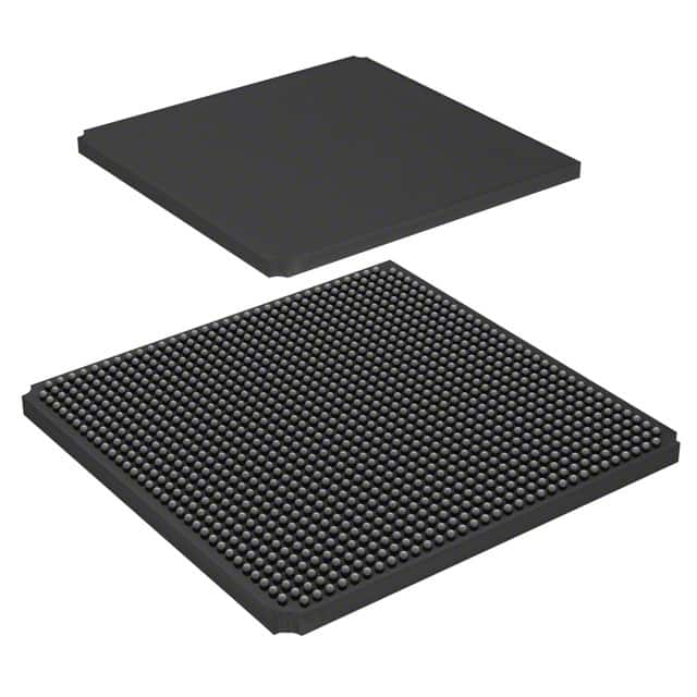
Package
The LFE2M70SE-5FN1152I comes in a compact package, suitable for surface mount technology (SMT) assembly.
Essence
The essence of the LFE2M70SE-5FN1152I lies in its ability to provide a customizable hardware solution for complex digital systems. It allows designers to implement their own logic functions and optimize performance according to specific requirements.
Packaging/Quantity
The LFE2M70SE-5FN1152I is typically packaged in reels or trays, with a quantity of 100 units per package.
Specifications
- FPGA Family: Lattice ECP2M
- Logic Elements: 70,000
- Embedded Memory: 1,152 Kbits
- Maximum User I/Os: 531
- Operating Voltage: 1.2V
- Speed Grade: -5
- Package Type: FN (Fine Pitch Ball Grid Array)
- Package Pins: 1152
Detailed Pin Configuration
The LFE2M70SE-5FN1152I has a total of 1152 pins, which are assigned to various functions such as input/output, clock signals, power supply, and configuration. The detailed pin configuration can be found in the product datasheet.
Functional Features
- High-speed performance: The LFE2M70SE-5FN1152I offers fast data processing capabilities, making it suitable for applications that require real-time operations.
- Reconfigurability: The FPGA can be reprogrammed multiple times, allowing for flexibility in adapting to changing system requirements.
- Low power consumption: The LFE2M70SE-5FN1152I is designed to minimize power consumption, making it energy-efficient and suitable for portable devices.
- Advanced connectivity: The FPGA supports various high-speed interfaces such as PCIe, Ethernet, and USB, enabling seamless integration with other components.
Advantages and Disadvantages
Advantages
- Customizability: The LFE2M70SE-5FN1152I allows designers to create tailored solutions for specific applications.
- High-performance: The FPGA offers excellent speed and processing capabilities.
- Flexibility: The reconfigurable nature of FPGAs enables quick prototyping and design iterations.
Disadvantages
- Complexity: Working with FPGAs requires specialized knowledge and expertise.
- Cost: FPGAs can be more expensive compared to other integrated circuits.
- Power consumption: While efforts have been made to reduce power consumption, FPGAs still consume more power compared to dedicated hardware solutions.
Working Principles
FPGAs consist of an array of programmable logic elements interconnected by configurable routing resources. These logic elements can be programmed to implement desired digital functions using a Hardware Description Language (HDL) or graphical tools. The LFE2M70SE-5FN1152I utilizes a combination of look-up tables, flip-flops, and interconnect resources to realize complex logic operations.
Detailed Application Field Plans
The LFE2M70SE-5FN1152I finds applications in various fields, including:
- Communications: Used in high-speed data transmission systems, network routers, and switches.
- Aerospace and Defense: Employed in radar systems, avionics, and secure communication systems.
- Industrial Automation: Utilized in control systems, robotics, and machine vision applications.
- Medical Devices: Integrated into medical imaging equipment, patient monitoring systems, and diagnostic instruments.
- Automotive: Applied in advanced driver-assistance systems (ADAS), infotainment systems, and engine control units.
Detailed and Complete Alternative Models
- Xilinx Virtex UltraScale+: A high-performance FPGA with advanced features and a wide range of configuration options.
- Intel Stratix 10: Offers exceptional performance and power efficiency for demanding applications.
- Microsemi PolarFire: Provides low-power consumption and security features suitable for industrial and automotive applications.
- QuickLogic EOS S3: A small form-factor FPGA designed for low-power edge computing and IoT applications.
These alternative models offer similar functionality to the LFE2M70SE-5FN1152I and can be considered based on specific project requirements.
Word count: 610 words
Seznam 10 běžných otázek a odpovědí souvisejících s aplikací LFE2M70SE-5FN1152I v technických řešeních
Sure! Here are 10 common questions and answers related to the application of LFE2M70SE-5FN1152I in technical solutions:
Q: What is LFE2M70SE-5FN1152I? A: LFE2M70SE-5FN1152I is a specific model of Field-Programmable Gate Array (FPGA) manufactured by Lattice Semiconductor.
Q: What are the key features of LFE2M70SE-5FN1152I? A: Some key features of LFE2M70SE-5FN1152I include 70,000 Look-Up Tables (LUTs), high-speed I/O interfaces, low power consumption, and support for various communication protocols.
Q: What are the typical applications of LFE2M70SE-5FN1152I? A: LFE2M70SE-5FN1152I is commonly used in applications such as telecommunications, industrial automation, automotive electronics, medical devices, and aerospace systems.
Q: How can LFE2M70SE-5FN1152I be programmed? A: LFE2M70SE-5FN1152I can be programmed using Hardware Description Languages (HDLs) like VHDL or Verilog, which describe the desired functionality of the FPGA.
Q: Can LFE2M70SE-5FN1152I be reprogrammed after deployment? A: Yes, LFE2M70SE-5FN1152I is a reprogrammable FPGA, allowing for updates and modifications to the design even after it has been deployed.
Q: What are the voltage requirements for LFE2M70SE-5FN1152I? A: LFE2M70SE-5FN1152I operates at a voltage range of 1.14V to 1.26V for core power, and 3.0V to 3.6V for I/O power.
Q: Does LFE2M70SE-5FN1152I support high-speed interfaces? A: Yes, LFE2M70SE-5FN1152I supports various high-speed interfaces such as DDR3/4 memory interfaces, PCIe, Ethernet, USB, and HDMI.
Q: What is the maximum operating frequency of LFE2M70SE-5FN1152I? A: The maximum operating frequency of LFE2M70SE-5FN1152I depends on the specific design and implementation, but it can typically reach several hundred megahertz (MHz) or even gigahertz (GHz).
Q: Are there any development tools available for LFE2M70SE-5FN1152I? A: Yes, Lattice Semiconductor provides development tools like Lattice Diamond or Lattice Radiant software suites for designing, simulating, and programming LFE2M70SE-5FN1152I.
Q: Where can I find more information about LFE2M70SE-5FN1152I? A: You can find more detailed information about LFE2M70SE-5FN1152I, including datasheets, application notes, and reference designs, on the official website of Lattice Semiconductor or by contacting their technical support team.