

Viz Specifikace pro podrobnosti o produktu.
LFE2M70SE-7F1152C
Product Overview
Category
The LFE2M70SE-7F1152C belongs to the category of Field Programmable Gate Arrays (FPGAs).
Use
This product is primarily used in digital logic circuits for various applications such as telecommunications, automotive, industrial automation, and consumer electronics.
Characteristics
- High-performance FPGA with advanced features
- Low power consumption
- Large capacity for complex designs
- Flexible and reprogrammable
- High-speed data processing capabilities
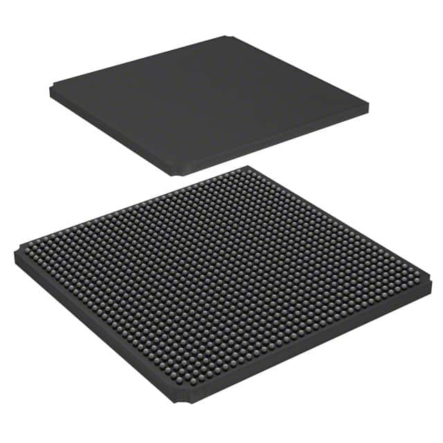
Package
The LFE2M70SE-7F1152C comes in a compact package that ensures easy integration into electronic systems. It is designed to be mounted on printed circuit boards (PCBs) using surface mount technology (SMT).
Essence
The essence of the LFE2M70SE-7F1152C lies in its ability to provide a customizable and versatile solution for implementing complex digital logic circuits.
Packaging/Quantity
This product is typically packaged in reels or trays, depending on the manufacturer's specifications. The quantity per package may vary, but it is commonly available in quantities suitable for both prototyping and production purposes.
Specifications
- FPGA Family: Lattice ECP2M
- Device Type: LFE2M70SE
- Logic Elements: 70,000
- Speed Grade: -7
- I/O Pins: 1,152
- Operating Voltage: 1.2V
- Package Type: FBGA
- Package Pins: 1152
- Temperature Range: -40°C to +100°C
Detailed Pin Configuration
The LFE2M70SE-7F1152C has a total of 1152 pins, which are assigned to various functions such as input/output (I/O), clock signals, power supply, and configuration. The pin configuration can be found in the product datasheet provided by the manufacturer.
Functional Features
- High-speed data processing: The LFE2M70SE-7F1152C offers fast data processing capabilities, making it suitable for applications that require real-time performance.
- Flexible reconfiguration: This FPGA allows for on-the-fly reprogramming, enabling dynamic changes to the logic circuitry without the need for hardware modifications.
- Low power consumption: The device is designed to operate efficiently with low power consumption, making it suitable for battery-powered applications.
- Extensive I/O capabilities: With 1152 I/O pins, the LFE2M70SE-7F1152C provides ample connectivity options for interfacing with external devices and peripherals.
- Large logic capacity: The FPGA's 70,000 logic elements provide sufficient resources for implementing complex digital designs.
Advantages and Disadvantages
Advantages
- Versatile and customizable solution for digital logic circuits
- High-performance capabilities
- Low power consumption
- Ample I/O options
- On-the-fly reconfiguration
Disadvantages
- Relatively high cost compared to other programmable logic devices
- Steeper learning curve for programming and design implementation
Working Principles
The LFE2M70SE-7F1152C operates based on the principles of configurable logic blocks (CLBs) and interconnect resources. The CLBs consist of look-up tables (LUTs), flip-flops, and other components that can be configured to implement desired logic functions. The interconnect resources allow for routing signals between different CLBs, enabling the creation of complex digital circuits.
Detailed Application Field Plans
The LFE2M70SE-7F1152C finds applications in various fields, including: - Telecommunications: Used in network equipment, base stations, and communication protocols. - Automotive: Employed in automotive electronics for control systems, driver assistance, and infotainment. - Industrial Automation: Utilized in programmable logic controllers (PLCs), motor control, and factory automation systems. - Consumer Electronics: Integrated into devices such as smartphones, tablets, and gaming consoles for enhanced functionality.
Detailed and Complete Alternative Models
- LFE2M70SE-6F1152C: Similar to the LFE2M70SE-7F1152C but with a different speed grade (-6).
- LFE2M70SE-5F1152C: Another variant with a lower speed grade (-5) but otherwise similar specifications.
- LFE2M70SE-8F1152C: Higher speed grade (-8) version of the LFE2M70SE series FPGA.
These alternative models offer different speed grades, allowing users to choose the one that best suits their specific requirements.
Word count: 611 words
Seznam 10 běžných otázek a odpovědí souvisejících s aplikací LFE2M70SE-7F1152C v technických řešeních
Sure! Here are 10 common questions and answers related to the application of LFE2M70SE-7F1152C in technical solutions:
Q: What is LFE2M70SE-7F1152C? A: LFE2M70SE-7F1152C is a specific model of Field-Programmable Gate Array (FPGA) manufactured by Lattice Semiconductor.
Q: What are the key features of LFE2M70SE-7F1152C? A: Some key features of LFE2M70SE-7F1152C include 70,000 Look-Up Tables (LUTs), 1,152 I/O pins, low power consumption, and high-speed performance.
Q: In what applications can LFE2M70SE-7F1152C be used? A: LFE2M70SE-7F1152C can be used in various applications such as telecommunications, industrial automation, automotive electronics, medical devices, and more.
Q: How can LFE2M70SE-7F1152C be programmed? A: LFE2M70SE-7F1152C can be programmed using hardware description languages (HDL) like VHDL or Verilog, or through graphical programming tools provided by Lattice Semiconductor.
Q: What is the power consumption of LFE2M70SE-7F1152C? A: The power consumption of LFE2M70SE-7F1152C depends on the specific design and usage scenario. It is generally known for its low power consumption capabilities.
Q: Can LFE2M70SE-7F1152C interface with other components or devices? A: Yes, LFE2M70SE-7F1152C can interface with other components or devices through its numerous I/O pins, supporting various communication protocols like UART, SPI, I2C, and more.
Q: What is the maximum operating frequency of LFE2M70SE-7F1152C? A: The maximum operating frequency of LFE2M70SE-7F1152C depends on the specific design and implementation. It can support high-speed operations up to several hundred megahertz.
Q: Can LFE2M70SE-7F1152C be reprogrammed after initial programming? A: Yes, LFE2M70SE-7F1152C is a reprogrammable FPGA, allowing for multiple programming cycles during the development and deployment stages.
Q: Are there any development tools available for LFE2M70SE-7F1152C? A: Yes, Lattice Semiconductor provides development tools like Lattice Diamond or Lattice Radiant, which offer design entry, synthesis, simulation, and programming capabilities for LFE2M70SE-7F1152C.
Q: Where can I find additional technical documentation and support for LFE2M70SE-7F1152C? A: You can find additional technical documentation, datasheets, application notes, and support resources on the official website of Lattice Semiconductor or by contacting their customer support team.
Please note that the answers provided here are general and may vary depending on the specific requirements and use cases of LFE2M70SE-7F1152C in different technical solutions.