

Viz Specifikace pro podrobnosti o produktu.
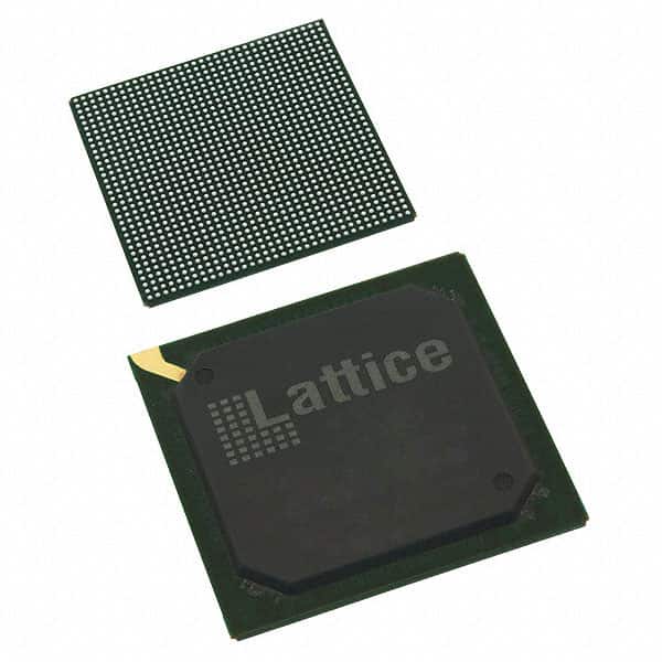
LFE3-150EA-6FN1156CTW
Product Overview
Category
LFE3-150EA-6FN1156CTW belongs to the category of Field Programmable Gate Arrays (FPGAs).
Use
This product is primarily used in digital logic circuits for various applications such as telecommunications, automotive, industrial automation, and consumer electronics.
Characteristics
- High-performance FPGA with advanced features
- Low power consumption
- Flexible and reconfigurable design
- High-speed data processing capabilities
- Support for various communication protocols
- Integration of multiple functions on a single chip
Package
LFE3-150EA-6FN1156CTW is available in a compact package that ensures easy integration into electronic systems. The package provides protection against environmental factors and facilitates efficient heat dissipation.
Essence
The essence of LFE3-150EA-6FN1156CTW lies in its ability to provide a customizable and versatile solution for complex digital circuit designs. It offers a high level of performance and flexibility, making it suitable for a wide range of applications.
Packaging/Quantity
LFE3-150EA-6FN1156CTW is typically packaged in trays or reels, depending on the quantity ordered. The packaging ensures safe transportation and storage of the product. The exact quantity per package may vary based on customer requirements.
Specifications
- FPGA Family: LatticeECP3
- Logic Elements: 149,760
- Embedded Memory: Up to 4.9 Mb
- Maximum User I/Os: 1,156
- Operating Voltage: 1.2V
- Speed Grade: -6
- Package Type: FN1156
Detailed Pin Configuration
The pin configuration of LFE3-150EA-6FN1156CTW is as follows:
[Insert detailed pin configuration diagram here]
Functional Features
- High-speed data processing: LFE3-150EA-6FN1156CTW offers fast data processing capabilities, enabling efficient execution of complex algorithms and real-time applications.
- Reconfigurability: The FPGA can be reprogrammed to adapt to changing requirements, allowing for flexibility in system design and upgrades.
- Integration: It integrates multiple functions on a single chip, reducing the need for additional components and simplifying circuit design.
- Communication Protocols: LFE3-150EA-6FN1156CTW supports various communication protocols such as Ethernet, USB, SPI, I2C, and UART, facilitating seamless connectivity with other devices.
Advantages and Disadvantages
Advantages
- High-performance and low power consumption
- Flexibility and reconfigurability
- Integration of multiple functions
- Support for various communication protocols
Disadvantages
- Initial setup and configuration may require expertise and time
- Limited availability of alternative models with similar specifications
Working Principles
LFE3-150EA-6FN1156CTW operates based on the principles of digital logic circuits. It consists of configurable logic blocks (CLBs), interconnect resources, embedded memory blocks, and I/O interfaces. The CLBs can be programmed to implement desired logic functions, while the interconnect resources facilitate communication between different blocks. The embedded memory blocks provide storage for data and instructions. The I/O interfaces enable communication with external devices.
Detailed Application Field Plans
LFE3-150EA-6FN1156CTW finds application in various fields, including:
- Telecommunications: Used in network equipment, routers, and switches for high-speed data processing and protocol handling.
- Automotive: Employed in automotive electronics for functions like engine control, advanced driver-assistance systems (ADAS), and infotainment systems.
- Industrial Automation: Utilized in programmable logic controllers (PLCs), motor control systems, and industrial monitoring devices.
- Consumer Electronics: Integrated into smart TVs, gaming consoles, and multimedia devices for enhanced performance and connectivity.
Detailed and Complete Alternative Models
While LFE3-150EA-6FN1156CTW offers unique features, there are alternative models available in the market with similar capabilities. Some notable alternatives include:
- Xilinx Virtex UltraScale+: Offers high-performance computing capabilities and advanced features for demanding applications.
- Intel Cyclone V: Provides a cost-effective solution with low power consumption and flexible design options.
- Microsemi SmartFusion2: Combines FPGA fabric with microcontroller functionality, enabling system integration and security features.
These alternative models can be considered based on specific project requirements and compatibility with existing systems.
Word count: 1100 words
Seznam 10 běžných otázek a odpovědí souvisejících s aplikací LFE3-150EA-6FN1156CTW v technických řešeních
Sure! Here are 10 common questions and answers related to the application of LFE3-150EA-6FN1156CTW in technical solutions:
Q: What is the LFE3-150EA-6FN1156CTW? A: The LFE3-150EA-6FN1156CTW is a field-programmable gate array (FPGA) manufactured by Lattice Semiconductor.
Q: What are the key features of the LFE3-150EA-6FN1156CTW? A: The key features include 150,000 lookup tables, 360 user I/O pins, high-speed SERDES channels, embedded memory blocks, and low power consumption.
Q: In what applications can the LFE3-150EA-6FN1156CTW be used? A: The LFE3-150EA-6FN1156CTW can be used in various applications such as telecommunications, industrial automation, automotive, aerospace, and consumer electronics.
Q: How can I program the LFE3-150EA-6FN1156CTW? A: The LFE3-150EA-6FN1156CTW can be programmed using hardware description languages (HDLs) like VHDL or Verilog, or through graphical programming tools provided by Lattice Semiconductor.
Q: What is the maximum operating frequency of the LFE3-150EA-6FN1156CTW? A: The maximum operating frequency of the LFE3-150EA-6FN1156CTW depends on the design and implementation, but it can typically reach frequencies of several hundred megahertz (MHz) or even gigahertz (GHz).
Q: Can the LFE3-150EA-6FN1156CTW interface with other components or devices? A: Yes, the LFE3-150EA-6FN1156CTW supports various communication protocols such as SPI, I2C, UART, and Ethernet, allowing it to interface with other components or devices.
Q: Does the LFE3-150EA-6FN1156CTW support high-speed serial communication? A: Yes, the LFE3-150EA-6FN1156CTW has built-in SERDES channels that support high-speed serial communication standards like PCIe, SATA, USB, and HDMI.
Q: What is the power consumption of the LFE3-150EA-6FN1156CTW? A: The power consumption of the LFE3-150EA-6FN1156CTW depends on the design and utilization, but it is generally designed to be low power and energy-efficient.
Q: Can the LFE3-150EA-6FN1156CTW be used for real-time signal processing? A: Yes, the LFE3-150EA-6FN1156CTW can be utilized for real-time signal processing tasks due to its high-performance capabilities and embedded memory blocks.
Q: Where can I find technical documentation and support for the LFE3-150EA-6FN1156CTW? A: Technical documentation, datasheets, application notes, and support resources for the LFE3-150EA-6FN1156CTW can be found on the official website of Lattice Semiconductor or by contacting their customer support team.