

Viz Specifikace pro podrobnosti o produktu.
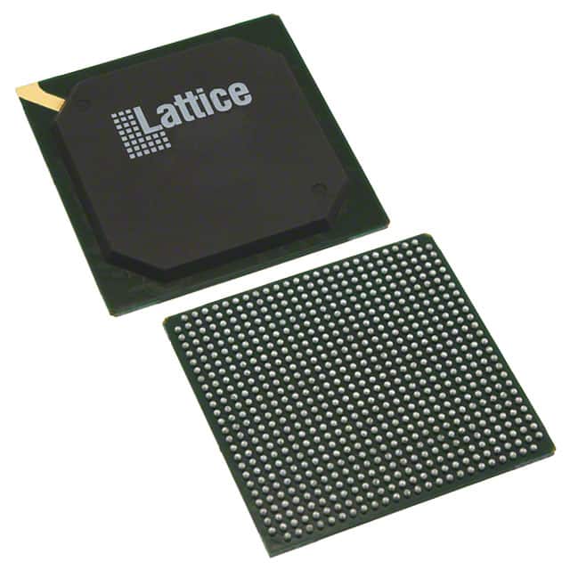
LFE3-150EA-8LFN672I
Product Overview
Category
The LFE3-150EA-8LFN672I belongs to the category of Field Programmable Gate Arrays (FPGAs).
Use
This FPGA is commonly used in various electronic devices and systems for digital logic implementation, such as communication equipment, industrial control systems, and high-performance computing.
Characteristics
- High-density programmable logic device
- Low power consumption
- High-speed performance
- Flexible and reconfigurable design
- Support for multiple I/O standards
- Advanced security features
Package
The LFE3-150EA-8LFN672I comes in a compact package that ensures easy integration into electronic circuits. It is designed to be surface-mounted on printed circuit boards (PCBs).
Essence
The essence of the LFE3-150EA-8LFN672I lies in its ability to provide a highly customizable and efficient solution for implementing complex digital logic functions in electronic systems.
Packaging/Quantity
This FPGA is typically packaged in reels or trays, depending on the manufacturer's specifications. The quantity per package may vary, but it is usually supplied in quantities suitable for production purposes.
Specifications
- Logic Elements: 150,000
- Embedded Memory: Up to 4.9 Mb
- DSP Blocks: 360
- Maximum User I/Os: 672
- Operating Voltage: 1.2V
- Operating Temperature Range: -40°C to 100°C
- Package Type: BGA (Ball Grid Array)
- Package Dimensions: 23mm x 23mm
Detailed Pin Configuration
The LFE3-150EA-8LFN672I has a total of 672 pins, which are assigned to various functions such as input, output, clock, and power supply. The pin configuration may vary depending on the specific application requirements and design considerations. For a detailed pin configuration diagram, please refer to the manufacturer's datasheet.
Functional Features
- High-speed performance: The LFE3-150EA-8LFN672I offers fast data processing capabilities, making it suitable for applications that require real-time operations.
- Reconfigurability: This FPGA allows users to modify the logic functions and interconnections even after the device has been programmed, providing flexibility in system design.
- Low power consumption: The LFE3-150EA-8LFN672I is designed to minimize power consumption, making it an energy-efficient choice for electronic systems.
- Advanced security features: This FPGA incorporates security mechanisms to protect sensitive information and prevent unauthorized access or tampering.
Advantages and Disadvantages
Advantages
- High-density programmable logic with a large number of logic elements and I/Os.
- Flexible and reconfigurable design enables customization and adaptability.
- Support for multiple I/O standards enhances compatibility with various interfaces.
- Low power consumption contributes to energy efficiency.
- Advanced security features provide protection against potential threats.
Disadvantages
- Complexity: Utilizing FPGAs requires expertise in digital design and programming.
- Cost: FPGAs can be more expensive compared to other integrated circuits due to their versatility and complexity.
- Design time: Developing complex designs for FPGAs may require significant time and effort.
Working Principles
The LFE3-150EA-8LFN672I operates based on the principles of configurable logic blocks (CLBs) and interconnect resources. CLBs consist of look-up tables (LUTs), flip-flops, and multiplexers, which can be configured to implement desired logic functions. Interconnect resources enable the routing of signals between different CLBs, allowing for the creation of complex digital circuits.
Detailed Application Field Plans
The LFE3-150EA-8LFN672I finds applications in various fields, including: - Communication equipment: Used for data processing, protocol handling, and signal modulation/demodulation. - Industrial control systems: Employed in automation, monitoring, and control of manufacturing processes. - High-performance computing: Utilized for parallel processing, data acceleration, and algorithm implementation.
Detailed and Complete Alternative Models
- LFE3-35EA-6FN484C
- LFE5U-45F-8BG381C
- LFXP2-5E-5TN144C
- LCMXO2-1200HC-4TG100C
These alternative models offer different specifications and features, catering to diverse application requirements. It is recommended to consult the manufacturer's documentation for detailed information on each model.
Word count: 650 words
Seznam 10 běžných otázek a odpovědí souvisejících s aplikací LFE3-150EA-8LFN672I v technických řešeních
Sure! Here are 10 common questions and answers related to the application of LFE3-150EA-8LFN672I in technical solutions:
Q: What is LFE3-150EA-8LFN672I? A: LFE3-150EA-8LFN672I is a specific model of Field-Programmable Gate Array (FPGA) manufactured by Lattice Semiconductor.
Q: What are the key features of LFE3-150EA-8LFN672I? A: Some key features of LFE3-150EA-8LFN672I include high-density programmable logic, embedded memory blocks, high-speed I/O interfaces, and low power consumption.
Q: What are the typical applications of LFE3-150EA-8LFN672I? A: LFE3-150EA-8LFN672I is commonly used in various technical solutions such as telecommunications, industrial automation, automotive electronics, medical devices, and aerospace systems.
Q: How can LFE3-150EA-8LFN672I be programmed? A: LFE3-150EA-8LFN672I can be programmed using Hardware Description Languages (HDLs) like VHDL or Verilog, which describe the desired functionality of the FPGA.
Q: Can LFE3-150EA-8LFN672I be reprogrammed after deployment? A: Yes, LFE3-150EA-8LFN672I is a reprogrammable FPGA, allowing for updates and modifications to the implemented logic even after deployment.
Q: What are the advantages of using LFE3-150EA-8LFN672I in technical solutions? A: Some advantages include flexibility, high performance, low power consumption, and the ability to implement complex digital systems in a single chip.
Q: Are there any limitations or considerations when using LFE3-150EA-8LFN672I? A: Some considerations include the need for expertise in FPGA programming, potential resource limitations based on the specific application requirements, and the cost of development tools.
Q: Can LFE3-150EA-8LFN672I interface with other electronic components or devices? A: Yes, LFE3-150EA-8LFN672I supports various I/O interfaces such as LVDS, DDR3, PCIe, Ethernet, and USB, allowing it to interface with other components or devices.
Q: Is technical support available for LFE3-150EA-8LFN672I? A: Yes, Lattice Semiconductor provides technical support for their products, including LFE3-150EA-8LFN672I, through their customer support channels.
Q: Where can I find more information about LFE3-150EA-8LFN672I and its application in technical solutions? A: You can find more detailed information, datasheets, reference designs, and application notes on the official website of Lattice Semiconductor or by contacting their sales representatives.