

Viz Specifikace pro podrobnosti o produktu.
LFE3-17EA-7MG328CAHQ
Product Overview
Category
The LFE3-17EA-7MG328CAHQ belongs to the category of Field Programmable Gate Arrays (FPGAs).
Use
This FPGA is commonly used in various electronic devices and systems for digital logic implementation, such as communication equipment, industrial control systems, and consumer electronics.
Characteristics
- High-performance programmable logic device
- Offers flexibility and reconfigurability
- Provides a large number of configurable logic blocks and input/output pins
- Supports complex digital circuit designs
- Enables rapid prototyping and development cycles
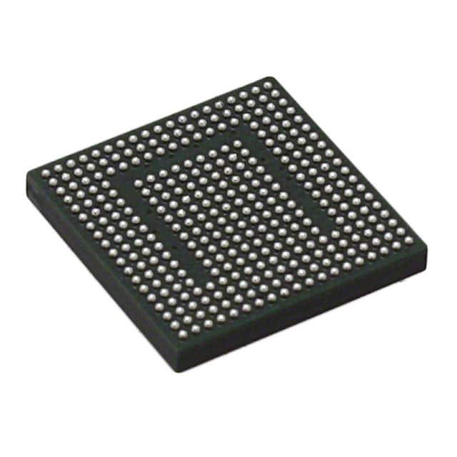
Package
The LFE3-17EA-7MG328CAHQ is available in a compact and durable package suitable for surface mount technology (SMT) assembly. The package ensures reliable electrical connections and protection against environmental factors.
Essence
The essence of the LFE3-17EA-7MG328CAHQ lies in its ability to provide a customizable and versatile platform for implementing digital logic circuits. It allows designers to create complex systems with high performance and adaptability.
Packaging/Quantity
The LFE3-17EA-7MG328CAHQ is typically packaged in reels or trays, depending on the manufacturer's specifications. The quantity per package may vary, but it is commonly available in quantities of 100 or more.
Specifications
- FPGA Family: Lattice ECP3
- Logic Elements: 17,280
- Memory Blocks: 328
- Maximum Number of I/O Pins: 328
- Operating Voltage: 1.2V
- Speed Grade: -7
- Package Type: BGA
- Package Pins: 484
Detailed Pin Configuration
The LFE3-17EA-7MG328CAHQ has a total of 328 I/O pins, which can be configured for various purposes. The pin configuration is as follows:
- Pin 1: VCCIO
- Pin 2: GND
- Pin 3: IOB33
- Pin 4: IOB32
- ...
- Pin 328: IOB1
Functional Features
- High-speed performance with low power consumption
- Configurable I/O standards and voltage levels
- Embedded memory blocks for efficient data storage
- Dedicated clock management resources for precise timing control
- Built-in DSP blocks for implementing complex mathematical operations
- Support for various communication protocols and interfaces
Advantages and Disadvantages
Advantages
- Flexibility and reconfigurability allow for rapid prototyping and design iterations
- High-performance capabilities enable the implementation of complex digital logic circuits
- Wide range of I/O pins and configurable I/O standards provide compatibility with different systems
- Low power consumption contributes to energy-efficient designs
Disadvantages
- Steep learning curve for beginners due to the complexity of FPGA programming
- Higher cost compared to fixed-function integrated circuits
- Limited availability of alternative models from other manufacturers
Working Principles
The LFE3-17EA-7MG328CAHQ operates based on the principles of field-programmable gate arrays. It consists of configurable logic blocks, input/output blocks, embedded memory blocks, and other specialized resources. These components can be interconnected and programmed to implement desired digital logic functions. The FPGA's internal routing resources allow for the creation of complex interconnections between different logic elements.
Detailed Application Field Plans
The LFE3-17EA-7MG328CAHQ finds applications in various fields, including:
Communication Equipment:
- Baseband processing in wireless communication systems
- Protocol conversion and signal conditioning
- Network packet processing and routing
Industrial Control Systems:
- Programmable logic controllers (PLCs)
- Motor control and motion systems
- Process automation and monitoring
Consumer Electronics:
- High-definition video processing
- Audio signal processing and enhancement
- Gaming consoles and graphics acceleration
Detailed and Complete Alternative Models
While the LFE3-17EA-7MG328CAHQ is a highly capable FPGA, there are alternative models available from different manufacturers that offer similar functionality. Some notable alternatives include:
- Xilinx Virtex-7 Series
- Intel (Altera) Cyclone V Series
- Microsemi SmartFusion2 Series
These alternative models provide comparable features and performance, allowing designers to choose the most suitable FPGA for their specific requirements.
Word count: 560 words
Seznam 10 běžných otázek a odpovědí souvisejících s aplikací LFE3-17EA-7MG328CAHQ v technických řešeních
Sure! Here are 10 common questions and answers related to the application of LFE3-17EA-7MG328CAHQ in technical solutions:
Q: What is the LFE3-17EA-7MG328CAHQ? A: The LFE3-17EA-7MG328CAHQ is a specific model of Field-Programmable Gate Array (FPGA) manufactured by Lattice Semiconductor.
Q: What are the key features of the LFE3-17EA-7MG328CAHQ? A: Some key features of this FPGA include 17,000 Look-Up Tables (LUTs), 328 I/O pins, and support for various communication protocols like PCIe, Ethernet, and USB.
Q: In what applications can the LFE3-17EA-7MG328CAHQ be used? A: This FPGA can be used in a wide range of applications such as industrial automation, telecommunications, automotive electronics, medical devices, and more.
Q: How can I program the LFE3-17EA-7MG328CAHQ? A: You can program this FPGA using hardware description languages (HDL) like VHDL or Verilog, along with design software provided by Lattice Semiconductor.
Q: Can I use the LFE3-17EA-7MG328CAHQ for high-speed data processing? A: Yes, this FPGA supports high-speed data processing with its built-in high-performance I/Os and dedicated DSP blocks.
Q: Does the LFE3-17EA-7MG328CAHQ have any security features? A: Yes, this FPGA offers security features like bitstream encryption and authentication to protect your intellectual property and prevent unauthorized access.
Q: Can I interface the LFE3-17EA-7MG328CAHQ with other components or devices? A: Absolutely! This FPGA has a wide range of I/O pins that can be used to interface with various components and devices, including sensors, actuators, memory modules, and more.
Q: What kind of power supply does the LFE3-17EA-7MG328CAHQ require? A: The LFE3-17EA-7MG328CAHQ typically requires a single 1.2V power supply, but it also supports multiple power domains for efficient power management.
Q: Can I reprogram the LFE3-17EA-7MG328CAHQ after deployment? A: Yes, this FPGA is field-programmable, which means you can reprogram it even after it has been deployed in your technical solution.
Q: Where can I find additional resources and support for the LFE3-17EA-7MG328CAHQ? A: You can find additional resources, documentation, and support on the official website of Lattice Semiconductor or by contacting their customer support team.
Please note that the specific details and answers may vary depending on the manufacturer's specifications and documentation.