

Viz Specifikace pro podrobnosti o produktu.
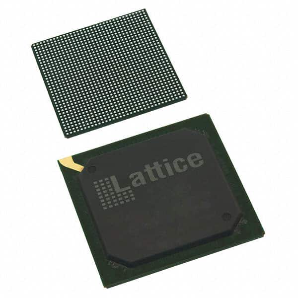
LFE3-70EA-6LFN1156C
Product Overview
Category
The LFE3-70EA-6LFN1156C belongs to the category of Field Programmable Gate Arrays (FPGAs).
Use
This FPGA is commonly used in electronic circuits for various applications such as digital signal processing, data communication, and embedded systems.
Characteristics
- High-performance programmable logic device
- Offers flexibility and reconfigurability
- Provides high-speed data processing capabilities
- Supports complex algorithms and computations
Package
The LFE3-70EA-6LFN1156C comes in a compact package that ensures easy integration into electronic circuit boards.
Essence
The essence of this FPGA lies in its ability to provide a customizable hardware platform that can be programmed to perform specific functions based on the user's requirements.
Packaging/Quantity
The LFE3-70EA-6LFN1156C is typically packaged individually and is available in varying quantities depending on the customer's needs.
Specifications
- Model: LFE3-70EA-6LFN1156C
- Logic Elements: 70,000
- Number of I/O Pins: 1,156
- Operating Voltage: 1.2V
- Maximum Frequency: 500 MHz
- Configuration Memory: 6 Mbits
- Package Type: BGA (Ball Grid Array)
- Temperature Range: -40°C to +100°C
Detailed Pin Configuration
The LFE3-70EA-6LFN1156C has a total of 1,156 pins, each serving a specific purpose in the overall functionality of the FPGA. The pin configuration includes input/output pins, power supply pins, clock pins, and configuration pins. A detailed pinout diagram can be found in the product datasheet.
Functional Features
- High-speed data processing capabilities
- Configurable logic elements for custom functionality
- Dedicated memory blocks for efficient storage and retrieval of data
- Built-in multipliers for complex arithmetic operations
- Flexible I/O interfaces for seamless integration with external devices
Advantages and Disadvantages
Advantages
- Flexibility and reconfigurability allow for quick prototyping and design iterations
- High-performance computing capabilities enable complex algorithms to be implemented efficiently
- Compact package size facilitates integration into space-constrained electronic systems
Disadvantages
- Steeper learning curve compared to traditional fixed-function integrated circuits
- Higher power consumption compared to dedicated application-specific integrated circuits (ASICs)
- Relatively higher cost per unit compared to mass-produced standard components
Working Principles
The LFE3-70EA-6LFN1156C operates based on the principles of digital logic. It consists of configurable logic elements, memory blocks, and I/O interfaces. The FPGA can be programmed using a Hardware Description Language (HDL) to define the desired functionality. Upon configuration, the FPGA executes the programmed logic, enabling it to perform specific tasks as required by the user.
Detailed Application Field Plans
The LFE3-70EA-6LFN1156C finds applications in various fields, including:
- Digital Signal Processing: Used in audio and video processing systems, image recognition, and compression algorithms.
- Communications: Employed in high-speed data communication systems, network routers, and switches.
- Embedded Systems: Integrated into automotive electronics, industrial control systems, and Internet of Things (IoT) devices.
Detailed and Complete Alternative Models
- Xilinx Virtex UltraScale+ VU9P: Offers higher logic capacity and faster performance.
- Intel Stratix 10 GX: Provides advanced features like high-speed transceivers and hardened floating-point units.
- Microsemi PolarFire FPGA: Known for its low power consumption and high-security features.
These alternative models offer similar functionality to the LFE3-70EA-6LFN1156C but may vary in terms of performance, capacity, and additional features.
In conclusion, the LFE3-70EA-6LFN1156C is a high-performance FPGA that offers flexibility, reconfigurability, and advanced computing capabilities. Its compact package and wide range of applications make it a versatile choice for various electronic systems.
Seznam 10 běžných otázek a odpovědí souvisejících s aplikací LFE3-70EA-6LFN1156C v technických řešeních
Sure! Here are 10 common questions and answers related to the application of LFE3-70EA-6LFN1156C in technical solutions:
Q: What is the LFE3-70EA-6LFN1156C? A: The LFE3-70EA-6LFN1156C is a field-programmable gate array (FPGA) manufactured by Lattice Semiconductor.
Q: What are the key features of the LFE3-70EA-6LFN1156C? A: Some key features include 70,000 Look-Up Tables (LUTs), high-speed I/O interfaces, embedded memory blocks, and low power consumption.
Q: What are the typical applications of the LFE3-70EA-6LFN1156C? A: The LFE3-70EA-6LFN1156C is commonly used in various applications such as telecommunications, industrial automation, automotive electronics, and medical devices.
Q: How can I program the LFE3-70EA-6LFN1156C? A: The LFE3-70EA-6LFN1156C can be programmed using hardware description languages (HDLs) like VHDL or Verilog, or through graphical programming tools provided by Lattice Semiconductor.
Q: What is the maximum operating frequency of the LFE3-70EA-6LFN1156C? A: The maximum operating frequency of the LFE3-70EA-6LFN1156C depends on the specific design and implementation, but it can typically reach several hundred megahertz (MHz).
Q: Can I interface the LFE3-70EA-6LFN1156C with other components or devices? A: Yes, the LFE3-70EA-6LFN1156C supports various I/O standards and can be easily interfaced with other components or devices such as sensors, memory modules, or communication interfaces.
Q: What is the power consumption of the LFE3-70EA-6LFN1156C? A: The power consumption of the LFE3-70EA-6LFN1156C depends on the specific design and utilization, but it generally operates at low power levels to optimize energy efficiency.
Q: Can the LFE3-70EA-6LFN1156C be reprogrammed after deployment? A: Yes, the LFE3-70EA-6LFN1156C is a reprogrammable FPGA, allowing for updates or modifications to the implemented logic even after deployment.
Q: Are there any development tools available for designing with the LFE3-70EA-6LFN1156C? A: Yes, Lattice Semiconductor provides a range of development tools, including software IDEs, simulation tools, and programming cables, to facilitate the design process with the LFE3-70EA-6LFN1156C.
Q: Where can I find technical documentation and support for the LFE3-70EA-6LFN1156C? A: Technical documentation, datasheets, application notes, and support resources for the LFE3-70EA-6LFN1156C can be found on the official website of Lattice Semiconductor or by contacting their customer support team.
Please note that the answers provided here are general and may vary depending on the specific requirements and use cases.