

Viz Specifikace pro podrobnosti o produktu.
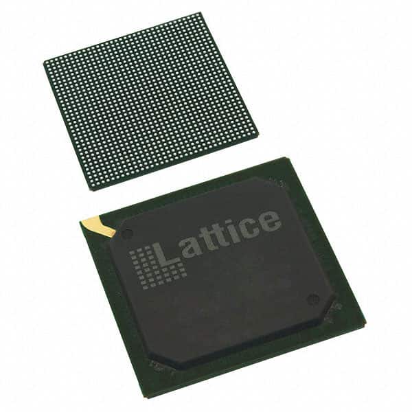
LFE3-70EA-7LFN1156C
Product Overview
Category
The LFE3-70EA-7LFN1156C belongs to the category of Field Programmable Gate Arrays (FPGAs).
Use
This FPGA is commonly used in various electronic devices and systems for digital logic implementation, such as communication equipment, industrial control systems, and consumer electronics.
Characteristics
- High-performance: The LFE3-70EA-7LFN1156C offers fast processing speeds and efficient resource utilization.
- Versatile: It supports a wide range of applications due to its flexible programmability.
- Low power consumption: This FPGA is designed to minimize power consumption, making it suitable for battery-powered devices.
- High-density integration: It provides a large number of configurable logic blocks, allowing complex designs to be implemented on a single chip.
Package
The LFE3-70EA-7LFN1156C comes in a compact package that ensures easy integration into circuit boards. It is available in a lead-free package, complying with environmental regulations.
Essence
The essence of the LFE3-70EA-7LFN1156C lies in its ability to provide a customizable hardware platform for implementing digital logic functions. It allows designers to create tailored solutions for specific applications without the need for custom silicon.
Packaging/Quantity
The LFE3-70EA-7LFN1156C is typically packaged in trays or reels, depending on the quantity ordered. The exact packaging and quantity can vary based on customer requirements.
Specifications
- Logic Elements: 70,000
- Embedded Memory: Up to 2,208 Kbits
- DSP Blocks: 360
- I/O Pins: 1,156
- Operating Voltage: 1.2V
- Maximum Frequency: 500 MHz
- Package Type: BGA (Ball Grid Array)
- Temperature Range: -40°C to 100°C
Detailed Pin Configuration
The LFE3-70EA-7LFN1156C has a total of 1,156 I/O pins. These pins are used for input and output connections with external devices. The pin configuration is detailed in the product datasheet provided by the manufacturer.
Functional Features
- High-speed performance: The LFE3-70EA-7LFN1156C offers fast processing capabilities, enabling real-time applications.
- Flexible I/O options: It provides a wide range of I/O standards, allowing compatibility with various communication protocols.
- Embedded memory: The FPGA includes embedded memory blocks that can be used for data storage or as lookup tables.
- DSP capabilities: With dedicated DSP blocks, it supports efficient implementation of digital signal processing algorithms.
- Clock management: The device incorporates clock management resources, enabling precise timing control.
Advantages and Disadvantages
Advantages
- Versatility: The LFE3-70EA-7LFN1156C can be programmed to perform different functions, making it suitable for diverse applications.
- Cost-effective: FPGAs eliminate the need for custom ASICs, reducing development costs and time-to-market.
- Reconfigurability: The ability to reprogram the FPGA allows for design modifications and upgrades without hardware changes.
- Integration: The high-density integration of logic elements and peripherals on a single chip simplifies system design.
Disadvantages
- Complexity: Designing for FPGAs requires expertise in hardware description languages and digital logic design.
- Power consumption: While efforts have been made to reduce power consumption, FPGAs still consume more power compared to dedicated ASICs.
- Limited performance optimization: FPGAs may not achieve the same level of performance as application-specific integrated circuits (ASICs) for certain applications.
Working Principles
The LFE3-70EA-7LFN1156C operates based on the principles of reconfigurable computing. It consists of an array of configurable logic blocks interconnected through programmable routing resources. The device can be programmed using hardware description languages (HDLs) to define the desired digital logic functions and interconnections.
During operation, the FPGA executes the programmed logic by routing signals through the configurable elements, such as look-up tables, flip-flops, and multiplexers. This allows for the implementation of complex digital circuits and systems.
Detailed Application Field Plans
The LFE3-70EA-7LFN1156C finds applications in various fields, including:
- Communication Systems: Used in wireless base stations, routers, and network switches for high-speed data processing and protocol handling.
- Industrial Control Systems: Employed in programmable logic controllers (PLCs) and automation systems for real-time control and monitoring.
- Consumer Electronics: Integrated into smart TVs, gaming consoles, and multimedia devices to enable advanced functionalities and connectivity.
- Medical Devices: Utilized in medical imaging equipment, patient monitoring
Seznam 10 běžných otázek a odpovědí souvisejících s aplikací LFE3-70EA-7LFN1156C v technických řešeních
Sure! Here are 10 common questions and answers related to the application of LFE3-70EA-7LFN1156C in technical solutions:
Q: What is the LFE3-70EA-7LFN1156C? A: The LFE3-70EA-7LFN1156C is a field-programmable gate array (FPGA) manufactured by Lattice Semiconductor.
Q: What are the key features of the LFE3-70EA-7LFN1156C? A: Some key features include 70,000 lookup tables (LUTs), 1,156 user I/O pins, high-speed SERDES channels, and low power consumption.
Q: What applications can the LFE3-70EA-7LFN1156C be used for? A: The LFE3-70EA-7LFN1156C can be used in various applications such as telecommunications, industrial automation, automotive electronics, and medical devices.
Q: How can I program the LFE3-70EA-7LFN1156C? A: The LFE3-70EA-7LFN1156C can be programmed using Lattice Diamond or Lattice Radiant software tools provided by Lattice Semiconductor.
Q: What is the power supply requirement for the LFE3-70EA-7LFN1156C? A: The LFE3-70EA-7LFN1156C requires a single power supply voltage of 1.2V.
Q: Can the LFE3-70EA-7LFN1156C support high-speed data transmission? A: Yes, the LFE3-70EA-7LFN1156C has built-in high-speed SERDES channels that support data rates up to 10 Gbps.
Q: Does the LFE3-70EA-7LFN1156C have any security features? A: Yes, the LFE3-70EA-7LFN1156C provides security features such as bitstream encryption and authentication to protect against unauthorized access.
Q: Can I use the LFE3-70EA-7LFN1156C in a battery-powered device? A: Yes, the LFE3-70EA-7LFN1156C is designed for low power consumption, making it suitable for battery-powered applications.
Q: What is the maximum operating temperature of the LFE3-70EA-7LFN1156C? A: The LFE3-70EA-7LFN1156C has a maximum junction temperature of 125°C.
Q: Are there any development boards available for the LFE3-70EA-7LFN1156C? A: Yes, Lattice Semiconductor offers development boards like the ECP5 Versa Evaluation Board that can be used with the LFE3-70EA-7LFN1156C for prototyping and testing.
Please note that the answers provided here are general and may vary depending on specific requirements and configurations.