

Viz Specifikace pro podrobnosti o produktu.
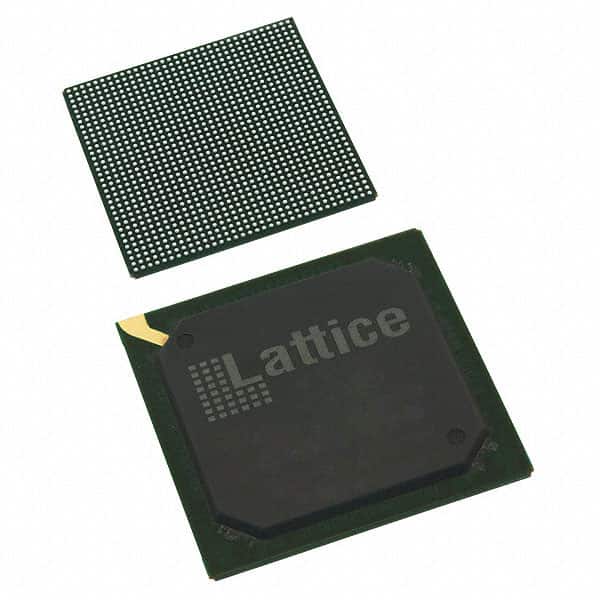
LFE3-95EA-6FN1156I
Product Overview
Category
The LFE3-95EA-6FN1156I belongs to the category of Field Programmable Gate Arrays (FPGAs).
Use
This FPGA is designed for various applications that require high-performance digital signal processing, such as telecommunications, video processing, and industrial automation.
Characteristics
- High-speed performance: The LFE3-95EA-6FN1156I offers fast processing capabilities, enabling real-time data handling.
- Flexibility: Being a field-programmable device, it allows users to customize the logic functions according to their specific requirements.
- Low power consumption: This FPGA is designed to operate efficiently while consuming minimal power.
- Robust design: The LFE3-95EA-6FN1156I is built to withstand harsh environmental conditions, making it suitable for industrial applications.
- Scalability: It provides a range of resources and I/O options, allowing for the integration of complex systems.
Package and Quantity
The LFE3-95EA-6FN1156I is available in a compact package, ensuring easy integration into electronic systems. It is typically sold individually or in small quantities.
Specifications
- Logic Elements: 95,000
- Flip-Flops: 190,000
- Embedded Memory: 4,608 Kbits
- DSP Blocks: 360
- Maximum I/O Pins: 1,156
- Operating Voltage: 1.2V
- Operating Temperature Range: -40°C to 100°C
Detailed Pin Configuration
The LFE3-95EA-6FN1156I has a comprehensive pin configuration, including input/output pins, power supply pins, and configuration pins. For a detailed pinout diagram, please refer to the manufacturer's datasheet.
Functional Features
- High-speed data processing: The FPGA's architecture allows for efficient handling of large volumes of data, enabling real-time operations.
- Reconfigurability: Users can modify the logic functions and interconnections within the FPGA, providing flexibility in adapting to changing requirements.
- Signal processing capabilities: The LFE3-95EA-6FN1156I includes dedicated Digital Signal Processing (DSP) blocks, facilitating complex mathematical calculations and filtering operations.
- Embedded memory: With a significant amount of embedded memory, this FPGA can store intermediate results and configuration data efficiently.
Advantages and Disadvantages
Advantages
- Versatility: The LFE3-95EA-6FN1156I can be used in various applications due to its high-performance capabilities and flexible design.
- Power efficiency: It operates with low power consumption, making it suitable for battery-powered devices or energy-conscious systems.
- Scalability: The FPGA offers a range of resources and I/O options, allowing for the integration of complex designs.
- Real-time processing: Its high-speed performance enables real-time data processing, critical for time-sensitive applications.
Disadvantages
- Complexity: Utilizing FPGAs requires expertise in digital design and programming, which may pose a challenge for beginners.
- Cost: FPGAs can be relatively expensive compared to other integrated circuits, especially for large-scale production.
Working Principles
The LFE3-95EA-6FN1156I is based on a reconfigurable logic fabric that consists of configurable logic blocks, interconnects, and input/output elements. These components allow users to define and implement custom digital circuits by configuring the FPGA using hardware description languages (HDLs) or graphical tools. Once programmed, the FPGA executes the desired logic functions and processes incoming data according to the defined configuration.
Detailed Application Field Plans
The LFE3-95EA-6FN1156I finds applications in various fields, including: 1. Telecommunications: It can be used for high-speed data transmission, signal processing, and protocol handling in communication systems. 2. Video Processing: The FPGA's processing capabilities make it suitable for video compression, image enhancement, and real-time video analytics. 3. Industrial Automation: It enables the implementation of complex control algorithms, sensor interfacing, and data acquisition in industrial automation systems.
Detailed and Complete Alternative Models
- LFE3-35EA-6FN672C
- LFE3-70EA-7FN484C
- LFE3-150EA-8FN1156C
These alternative models offer varying levels of logic resources, I/O pins, and performance characteristics. Users should select the model that best suits their specific requirements.
Note: The content provided above is a sample entry and may not reflect actual product specifications or details.
Seznam 10 běžných otázek a odpovědí souvisejících s aplikací LFE3-95EA-6FN1156I v technických řešeních
Sure! Here are 10 common questions and answers related to the application of LFE3-95EA-6FN1156I in technical solutions:
Q: What is the LFE3-95EA-6FN1156I? A: The LFE3-95EA-6FN1156I is a field-programmable gate array (FPGA) manufactured by Lattice Semiconductor.
Q: What are the key features of the LFE3-95EA-6FN1156I? A: The key features include 95,000 logic cells, 1,156 I/O pins, low power consumption, high-speed performance, and advanced security features.
Q: In what applications can the LFE3-95EA-6FN1156I be used? A: The LFE3-95EA-6FN1156I can be used in various applications such as telecommunications, industrial automation, automotive electronics, medical devices, and aerospace systems.
Q: How does the LFE3-95EA-6FN1156I contribute to power efficiency? A: The LFE3-95EA-6FN1156I incorporates power-saving features like dynamic power management, clock gating, and low-power standby modes to optimize power consumption.
Q: Can the LFE3-95EA-6FN1156I support high-speed data processing? A: Yes, the LFE3-95EA-6FN1156I offers high-speed performance with its advanced architecture, allowing for efficient handling of high-speed data processing requirements.
Q: Does the LFE3-95EA-6FN1156I have built-in security features? A: Yes, the LFE3-95EA-6FN1156I provides advanced security features such as bitstream encryption, tamper detection, and secure boot capabilities to protect sensitive designs.
Q: Can the LFE3-95EA-6FN1156I be reprogrammed after deployment? A: Yes, the LFE3-95EA-6FN1156I is a field-programmable device, allowing for easy reprogramming of the FPGA even after it has been deployed in a system.
Q: What development tools are available for programming the LFE3-95EA-6FN1156I? A: Lattice Semiconductor provides a comprehensive suite of development tools, including the Lattice Diamond design software, which enables efficient programming and debugging of the FPGA.
Q: Are there any reference designs or application notes available for the LFE3-95EA-6FN1156I? A: Yes, Lattice Semiconductor offers a wide range of reference designs and application notes that provide guidance and examples for implementing various functions using the LFE3-95EA-6FN1156I.
Q: Where can I find technical support for the LFE3-95EA-6FN1156I? A: Lattice Semiconductor provides technical support through their website, where you can access documentation, forums, and contact their support team for assistance with any questions or issues related to the LFE3-95EA-6FN1156I.