

Viz Specifikace pro podrobnosti o produktu.
LFE5UM-85F-6BG381C
Product Overview
Category
The LFE5UM-85F-6BG381C belongs to the category of Field Programmable Gate Arrays (FPGAs).
Use
This FPGA is commonly used in various electronic devices and systems for digital logic implementation, such as communication equipment, industrial control systems, and consumer electronics.
Characteristics
- High-performance FPGA with advanced features
- Low power consumption
- Large capacity for complex designs
- Flexible and reprogrammable
- Supports a wide range of applications
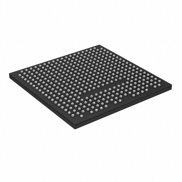
Package
The LFE5UM-85F-6BG381C comes in a compact and durable package that ensures protection during handling and installation. The package is designed to withstand harsh environmental conditions.
Essence
The essence of the LFE5UM-85F-6BG381C lies in its ability to provide a customizable and versatile solution for implementing digital logic circuits. It offers high performance and flexibility, making it suitable for a wide range of applications.
Packaging/Quantity
The LFE5UM-85F-6BG381C is typically packaged individually and is available in various quantities depending on the requirements of the customer or project.
Specifications
- Model: LFE5UM-85F-6BG381C
- Logic Elements: 85,000
- Block RAM: 6,000 Kbits
- Package: BGA381
- Operating Voltage: 1.2V
- Maximum Frequency: 500 MHz
- I/O Pins: 381
- Configuration Memory: Flash-based
Detailed Pin Configuration
The LFE5UM-85F-6BG381C has a total of 381 I/O pins, which are used for input and output connections. These pins are arranged in a specific configuration to facilitate easy integration into various electronic systems.
For a detailed pin configuration diagram, please refer to the manufacturer's datasheet or documentation.
Functional Features
- High-speed performance: The LFE5UM-85F-6BG381C operates at a maximum frequency of 500 MHz, allowing for efficient execution of complex digital logic designs.
- Low power consumption: This FPGA is designed to minimize power consumption, making it suitable for battery-powered devices and energy-efficient applications.
- Flexible I/O options: With 381 I/O pins, the LFE5UM-85F-6BG381C provides ample connectivity options for interfacing with other components and systems.
- Large capacity: The FPGA offers 85,000 logic elements and 6,000 Kbits of block RAM, enabling the implementation of complex designs.
Advantages and Disadvantages
Advantages
- Versatile and customizable solution for digital logic implementation
- High-performance capabilities
- Low power consumption
- Ample I/O options for connectivity
- Large capacity for complex designs
Disadvantages
- May require specialized knowledge and expertise for programming and configuration
- Initial setup and development time may be longer compared to off-the-shelf solutions
Working Principles
The LFE5UM-85F-6BG381C works based on the principles of field-programmable gate arrays. It consists of configurable logic blocks (CLBs), interconnect resources, and I/O blocks. The CLBs can be programmed to implement various digital logic functions, while the interconnect resources enable communication between different blocks. The I/O blocks facilitate input and output connections with external devices.
The FPGA's working principle involves configuring the logic elements and interconnections using a hardware description language (HDL) or a graphical design tool. Once programmed, the FPGA executes the desired digital logic operations based on the configured design.
Detailed Application Field Plans
The LFE5UM-85F-6BG381C finds applications in various fields, including:
- Communication Equipment: Used in networking devices, routers, and switches for high-speed data processing and protocol handling.
- Industrial Control Systems: Employed in automation systems, robotics, and control panels to implement complex control algorithms and interface with sensors and actuators.
- Consumer Electronics: Integrated into smart TVs, gaming consoles, and multimedia devices for video and audio processing, as well as user interface implementation.
Detailed and Complete Alternative Models
- LFE5UM-45F-8BG381C: A similar FPGA model with a lower logic element count but higher block RAM capacity.
- LFE5UM-120F-9BG381C: An alternative FPGA model with a higher logic element count and increased I/O pin count.
- LFE5UM-25F-12BG381C: A compact FPGA model with a lower logic element count, suitable for space-constrained applications.
Please note that the above alternative models are just a few examples, and there are many other options available in the market with varying specifications and features.
*Word count:
Seznam 10 běžných otázek a odpovědí souvisejících s aplikací LFE5UM-85F-6BG381C v technických řešeních
Sure! Here are 10 common questions and answers related to the application of LFE5UM-85F-6BG381C in technical solutions:
Q: What is the LFE5UM-85F-6BG381C? A: The LFE5UM-85F-6BG381C is a high-performance field-programmable gate array (FPGA) manufactured by Lattice Semiconductor.
Q: What are the key features of the LFE5UM-85F-6BG381C? A: The key features include a large number of logic elements, high-speed transceivers, embedded memory blocks, and support for various I/O standards.
Q: What are some typical applications of the LFE5UM-85F-6BG381C? A: The LFE5UM-85F-6BG381C is commonly used in applications such as telecommunications, networking, industrial automation, video processing, and high-performance computing.
Q: How can I program the LFE5UM-85F-6BG381C? A: The LFE5UM-85F-6BG381C can be programmed using Lattice Diamond or Lattice Radiant software tools, which provide a graphical interface for designing and configuring the FPGA.
Q: What is the power supply requirement for the LFE5UM-85F-6BG381C? A: The LFE5UM-85F-6BG381C requires a single 1.2V core voltage supply and a separate 3.3V auxiliary voltage supply.
Q: Can I interface the LFE5UM-85F-6BG381C with other components or devices? A: Yes, the LFE5UM-85F-6BG381C supports various I/O standards, including LVCMOS, LVTTL, LVDS, and differential signaling, allowing easy interfacing with other components or devices.
Q: What is the maximum operating frequency of the LFE5UM-85F-6BG381C? A: The LFE5UM-85F-6BG381C can operate at frequencies up to 1.6 GHz, depending on the design and implementation.
Q: Does the LFE5UM-85F-6BG381C have built-in memory? A: Yes, the LFE5UM-85F-6BG381C has embedded memory blocks (RAM) that can be used for storing data or implementing memory-intensive functions.
Q: Can I use the LFE5UM-85F-6BG381C for real-time signal processing? A: Yes, the high-speed transceivers and configurable logic elements of the LFE5UM-85F-6BG381C make it suitable for real-time signal processing applications.
Q: Are there any development boards available for the LFE5UM-85F-6BG381C? A: Yes, Lattice Semiconductor offers development boards specifically designed for the LFE5UM-85F-6BG381C, which provide a convenient platform for prototyping and testing your designs.
Please note that these answers are general and may vary depending on specific requirements and application scenarios.