

Viz Specifikace pro podrobnosti o produktu.
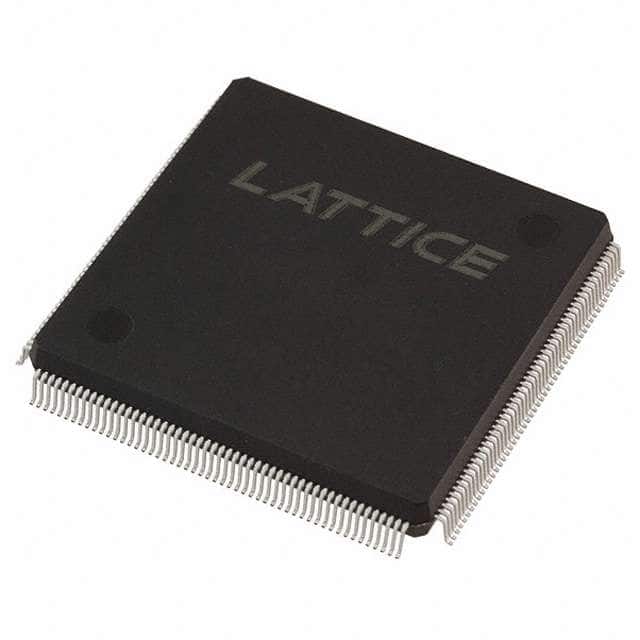
LFEC1E-3QN208C
Product Overview
Category
LFEC1E-3QN208C belongs to the category of Field-Programmable Gate Arrays (FPGAs).
Use
This product is primarily used in digital logic circuits for various applications such as telecommunications, automotive, aerospace, and consumer electronics.
Characteristics
- High-performance programmable logic device
- Offers flexibility in designing complex digital systems
- Provides reconfigurability for rapid prototyping and system development
Package
LFEC1E-3QN208C comes in a compact Quad Flat No-Lead (QFN) package.
Essence
The essence of LFEC1E-3QN208C lies in its ability to provide a customizable and versatile solution for implementing digital logic designs.
Packaging/Quantity
Each package of LFEC1E-3QN208C contains one unit of the FPGA.
Specifications
- Device Type: Field-Programmable Gate Array
- Model Number: LFEC1E-3QN208C
- Package Type: QFN
- Operating Temperature Range: -40°C to 85°C
- Logic Elements: 1,500
- I/O Pins: 208
- Power Supply Voltage: 1.2V
Detailed Pin Configuration
The pin configuration of LFEC1E-3QN208C is as follows:
- Pin 1: VCCIO
- Pin 2: GND
- Pin 3: IOB_0
- Pin 4: IOB_1
- ...
- Pin 208: IOB_206
Functional Features
- High-speed performance
- Low power consumption
- Configurable I/O standards
- Embedded memory blocks
- Clock management resources
- Built-in security features
Advantages and Disadvantages
Advantages
- Flexibility in design and reconfiguration
- Faster time-to-market for digital systems
- Cost-effective compared to custom ASICs
- Suitable for prototyping and low-volume production
Disadvantages
- Limited scalability for large-scale designs
- Higher power consumption compared to dedicated ASICs
- Steeper learning curve for beginners
Working Principles
LFEC1E-3QN208C operates based on the principles of field-programmable gate arrays. It consists of configurable logic blocks, programmable interconnects, and I/O elements. The device can be programmed using hardware description languages (HDL) such as VHDL or Verilog to implement desired digital logic functions.
Detailed Application Field Plans
LFEC1E-3QN208C finds applications in various fields, including:
- Telecommunications: Used in network routers, switches, and communication protocols.
- Automotive: Employed in automotive control systems, driver assistance systems, and infotainment systems.
- Aerospace: Utilized in avionics, satellite communication systems, and flight control systems.
- Consumer Electronics: Integrated into smartphones, tablets, gaming consoles, and multimedia devices.
Detailed and Complete Alternative Models
Some alternative models to LFEC1E-3QN208C include:
- LFE5U-45F-8BG381C
- LFXP6C-4TN144C
- LCMXO2-1200HC-4TG100C
- XC7A35T-1CPG236C
These models offer similar functionalities and can be considered as alternatives depending on specific requirements.
Word count: 410 words
Seznam 10 běžných otázek a odpovědí souvisejících s aplikací LFEC1E-3QN208C v technických řešeních
Sure! Here are 10 common questions and answers related to the application of LFEC1E-3QN208C in technical solutions:
Q1: What is LFEC1E-3QN208C? A1: LFEC1E-3QN208C is a specific model of Field-Programmable Gate Array (FPGA) manufactured by a company called Lattice Semiconductor.
Q2: What is an FPGA? A2: FPGA stands for Field-Programmable Gate Array. It is a type of integrated circuit that can be programmed after manufacturing to perform specific functions.
Q3: What are the key features of LFEC1E-3QN208C? A3: LFEC1E-3QN208C has 1,200 Look-Up Tables (LUTs), 3,000 flip-flops, and 208 pins. It operates at a voltage of 3.3V and supports various I/O standards.
Q4: What are some typical applications of LFEC1E-3QN208C? A4: LFEC1E-3QN208C is commonly used in applications such as industrial automation, automotive electronics, telecommunications, medical devices, and consumer electronics.
Q5: How can LFEC1E-3QN208C be programmed? A5: LFEC1E-3QN208C can be programmed using Hardware Description Languages (HDLs) like VHDL or Verilog, or through graphical programming tools provided by Lattice Semiconductor.
Q6: Can LFEC1E-3QN208C be reprogrammed multiple times? A6: Yes, LFEC1E-3QN208C is a reprogrammable FPGA, which means it can be reprogrammed multiple times to change its functionality.
Q7: What are the advantages of using LFEC1E-3QN208C in technical solutions? A7: Some advantages include its flexibility, high-performance capabilities, low power consumption, and the ability to implement complex logic functions.
Q8: Are there any limitations or considerations when using LFEC1E-3QN208C? A8: Some considerations include the need for expertise in FPGA programming, potential design constraints, and the cost associated with using FPGAs compared to other solutions.
Q9: Can LFEC1E-3QN208C interface with other components or devices? A9: Yes, LFEC1E-3QN208C can interface with various components and devices through its I/O pins, supporting different communication protocols like SPI, I2C, UART, etc.
Q10: Where can I find more information about LFEC1E-3QN208C and its application in technical solutions? A10: You can refer to the datasheet and technical documentation provided by Lattice Semiconductor. Additionally, online forums and communities dedicated to FPGA programming can be helpful resources.