

Viz Specifikace pro podrobnosti o produktu.
LFXP2-8E-6FTN256C
Product Overview
Category
The LFXP2-8E-6FTN256C belongs to the category of Field-Programmable Gate Arrays (FPGAs).
Use
FPGAs are integrated circuits that can be programmed after manufacturing. The LFXP2-8E-6FTN256C is specifically designed for applications requiring high-performance and low-power consumption.
Characteristics
- High performance: The LFXP2-8E-6FTN256C offers a high logic density, allowing for complex designs and efficient processing.
- Low power consumption: This FPGA is designed to minimize power usage, making it suitable for battery-powered devices.
- Flexible configuration: The LFXP2-8E-6FTN256C can be reprogrammed multiple times, enabling rapid prototyping and design iterations.
- Small package size: The compact form factor of this FPGA makes it suitable for space-constrained applications.
Package and Quantity
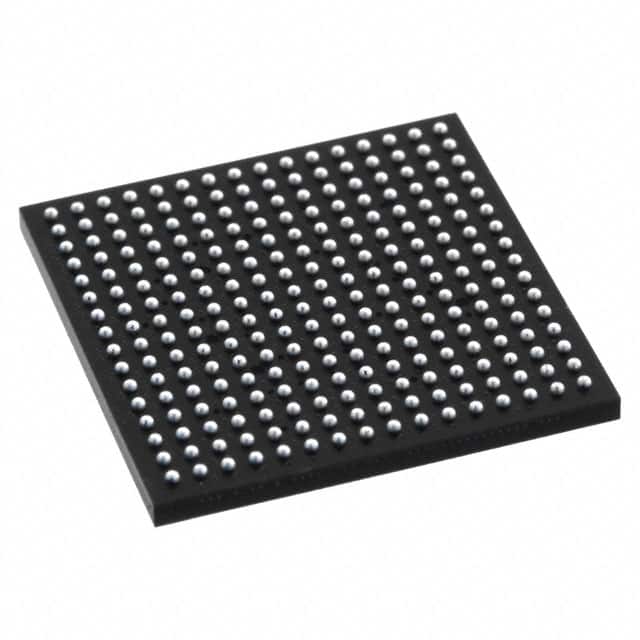
The LFXP2-8E-6FTN256C is available in a 256-pin Fine-Pitch Ball Grid Array (FBGA) package. It is typically sold individually or in small quantities.
Specifications
- Logic elements: 8,000
- Flip-flops: 4,000
- Embedded memory: 288 Kbits
- Maximum user I/Os: 162
- Operating voltage: 1.2V
- Operating temperature range: -40°C to 100°C
- Package dimensions: 17mm x 17mm
Detailed Pin Configuration
The LFXP2-8E-6FTN256C has a total of 256 pins. These pins are used for various purposes, including input/output connections, power supply, and configuration.
For a detailed pin configuration diagram, please refer to the manufacturer's datasheet.
Functional Features
- High-speed performance: The LFXP2-8E-6FTN256C offers fast processing capabilities, making it suitable for applications requiring real-time data processing.
- Flexible I/O options: This FPGA provides a wide range of I/O standards, allowing for seamless integration with different devices and protocols.
- Built-in memory: The embedded memory blocks enable efficient storage and retrieval of data within the FPGA itself.
- Configurable logic: The LFXP2-8E-6FTN256C allows users to define their own logic functions, providing flexibility in implementing custom designs.
Advantages and Disadvantages
Advantages
- High-performance processing capabilities
- Low power consumption
- Compact form factor
- Flexible configuration options
Disadvantages
- Limited number of user I/Os
- Relatively small embedded memory compared to other FPGAs in its class
Working Principles
The LFXP2-8E-6FTN256C operates based on the principles of reconfigurable computing. It consists of an array of configurable logic blocks interconnected through programmable routing resources. These logic blocks can be programmed to implement various digital circuits and functions.
The FPGA can be configured using a hardware description language (HDL) or a graphical design tool. Once programmed, the FPGA executes the desired logic functions, enabling the device to perform specific tasks.
Detailed Application Field Plans
The LFXP2-8E-6FTN256C finds applications in various fields, including:
- Communications: Used in networking equipment, routers, and switches for high-speed data processing.
- Industrial automation: Enables control and monitoring of complex systems in manufacturing plants.
- Aerospace and defense: Utilized in radar systems, avionics, and military-grade communication devices.
- Medical devices: Provides processing capabilities for medical imaging, patient monitoring, and diagnostic equipment.
- Internet of Things (IoT): Supports edge computing and data processing in IoT devices.
Detailed and Complete Alternative Models
- LFXP2-5E-6FTN256C: Similar to the LFXP2-8E-6FTN256C but with a lower logic element count.
- LFXP2-12E-6FTN256C: Offers higher logic density compared to the LFXP2-8E-6FTN256C.
- LFXP2-17E-6FTN256C: Provides even higher logic capacity for more complex designs.
These alternative models offer varying levels of performance and logic density, allowing users to choose the most suitable FPGA for their specific requirements.
In conclusion, the LFXP2-8E-6FTN256C is a high-performance and low-power FPGA that offers flexibility and compactness. With its wide range of applications and availability of alternative models, it serves as a versatile solution for various digital design needs.
Seznam 10 běžných otázek a odpovědí souvisejících s aplikací LFXP2-8E-6FTN256C v technických řešeních
Sure! Here are 10 common questions and answers related to the application of LFXP2-8E-6FTN256C in technical solutions:
Q: What is the LFXP2-8E-6FTN256C? A: The LFXP2-8E-6FTN256C is a field-programmable gate array (FPGA) manufactured by Lattice Semiconductor.
Q: What are the key features of the LFXP2-8E-6FTN256C? A: The key features of this FPGA include 8,000 Look-Up Tables (LUTs), 256 I/O pins, low power consumption, and high-speed performance.
Q: What are some typical applications of the LFXP2-8E-6FTN256C? A: This FPGA is commonly used in various applications such as industrial automation, telecommunications, automotive electronics, and consumer electronics.
Q: How can I program the LFXP2-8E-6FTN256C? A: The LFXP2-8E-6FTN256C can be programmed using Lattice Diamond or Lattice Radiant software tools provided by Lattice Semiconductor.
Q: What is the maximum operating frequency of the LFXP2-8E-6FTN256C? A: The maximum operating frequency of this FPGA is typically around 400 MHz, depending on the design and implementation.
Q: Can I interface the LFXP2-8E-6FTN256C with other components or devices? A: Yes, the LFXP2-8E-6FTN256C supports various standard interfaces such as SPI, I2C, UART, and GPIO, allowing easy integration with other components or devices.
Q: Does the LFXP2-8E-6FTN256C support high-speed serial communication protocols? A: Yes, this FPGA supports high-speed serial protocols like PCIe, Gigabit Ethernet, and USB, making it suitable for applications requiring fast data transfer.
Q: What is the power supply requirement for the LFXP2-8E-6FTN256C? A: The LFXP2-8E-6FTN256C typically operates at a voltage range of 1.2V to 3.3V, depending on the specific design requirements.
Q: Can I reprogram the LFXP2-8E-6FTN256C in the field after deployment? A: Yes, the LFXP2-8E-6FTN256C is a field-programmable device, meaning you can reprogram it even after it has been deployed in a system.
Q: Are there any development boards or evaluation kits available for the LFXP2-8E-6FTN256C? A: Yes, Lattice Semiconductor provides development boards and evaluation kits specifically designed for the LFXP2-8E-6FTN256C, which can help in prototyping and testing your designs.
Please note that the answers provided here are general and may vary based on specific design requirements and application scenarios.