

Viz Specifikace pro podrobnosti o produktu.
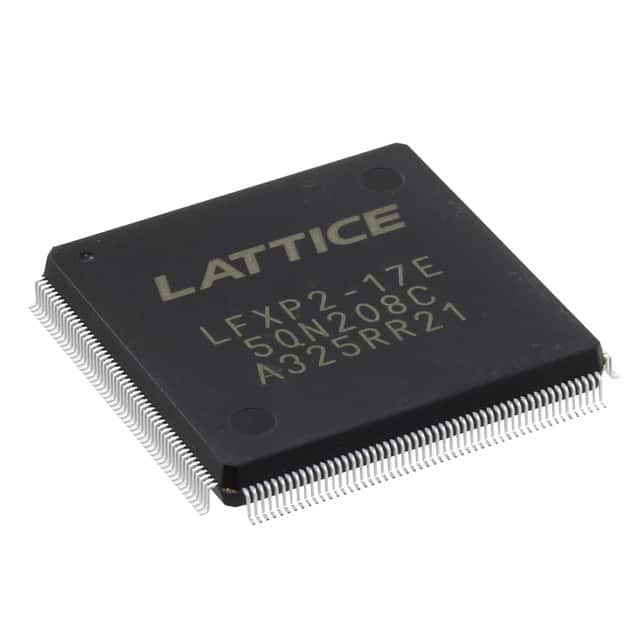
LFXP2-8E-6QN208I
Product Overview
Category
The LFXP2-8E-6QN208I belongs to the category of Field-Programmable Gate Arrays (FPGAs).
Use
This FPGA is commonly used in electronic circuits for various applications, including digital signal processing, telecommunications, automotive electronics, and industrial automation.
Characteristics
- High-performance programmable logic device
- Low power consumption
- Compact size
- Versatile functionality
- Reliable performance
Package
The LFXP2-8E-6QN208I comes in a compact Quad Flat No-Lead (QFN) package.
Essence
The essence of this FPGA lies in its ability to be programmed and reconfigured to perform specific functions, making it highly adaptable for different applications.
Packaging/Quantity
The LFXP2-8E-6QN208I is typically packaged individually and is available in various quantities depending on the manufacturer's specifications.
Specifications
- Logic Cells: 8,000
- Look-Up Tables (LUTs): 16,000
- Flip-Flops: 32,000
- Block RAM: 360 Kbits
- Maximum Frequency: 400 MHz
- I/O Pins: 208
- Voltage Range: 1.2V - 3.3V
- Operating Temperature Range: -40°C to 100°C
Detailed Pin Configuration
The LFXP2-8E-6QN208I has a total of 208 pins, each serving a specific purpose within the FPGA's architecture. The detailed pin configuration can be found in the product datasheet provided by the manufacturer.
Functional Features
- High-speed data processing capabilities
- Configurable I/O standards
- Embedded memory blocks for efficient data storage
- Flexible clock management resources
- Support for various communication protocols
- On-chip debugging features
Advantages and Disadvantages
Advantages
- Flexibility in design and reconfiguration
- High-performance computing capabilities
- Low power consumption
- Compact size
- Wide range of I/O options
- Cost-effective solution compared to custom ASICs
Disadvantages
- Steeper learning curve for programming and utilization
- Limited resources compared to larger FPGAs
- Higher cost compared to microcontrollers for simpler applications
Working Principles
The LFXP2-8E-6QN208I operates based on the principles of digital logic. It consists of configurable logic blocks, interconnects, and input/output elements. The FPGA can be programmed using Hardware Description Languages (HDL) such as VHDL or Verilog, allowing designers to define the desired functionality and interconnections within the device.
Detailed Application Field Plans
The LFXP2-8E-6QN208I finds extensive use in various application fields, including:
- Digital Signal Processing: Used for real-time audio and video processing, image recognition, and compression algorithms.
- Telecommunications: Employed in network routers, switches, and base stations for high-speed data processing and protocol handling.
- Automotive Electronics: Utilized in automotive control systems, driver assistance systems, and infotainment systems.
- Industrial Automation: Integrated into programmable logic controllers (PLCs), motor control systems, and industrial monitoring equipment.
Detailed and Complete Alternative Models
- Xilinx Spartan-6 XC6SLX9: Offers similar performance and features with a smaller logic capacity.
- Altera Cyclone IV EP4CE6: Provides comparable functionality at a lower price point.
- Microsemi SmartFusion2 M2S010: Combines FPGA fabric with a microcontroller core for enhanced system integration.
These alternative models can be considered based on specific project requirements and constraints.
Word count: 512 words
Seznam 10 běžných otázek a odpovědí souvisejících s aplikací LFXP2-8E-6QN208I v technických řešeních
Sure! Here are 10 common questions and answers related to the application of LFXP2-8E-6QN208I in technical solutions:
Q: What is the LFXP2-8E-6QN208I? A: The LFXP2-8E-6QN208I is a field-programmable gate array (FPGA) manufactured by Lattice Semiconductor.
Q: What are the key features of the LFXP2-8E-6QN208I? A: The key features include 8,000 Look-Up Tables (LUTs), 208-pin QFN package, 6-input look-up tables, and low power consumption.
Q: What are some typical applications for the LFXP2-8E-6QN208I? A: The LFXP2-8E-6QN208I is commonly used in applications such as industrial automation, automotive electronics, consumer electronics, and telecommunications.
Q: How can I program the LFXP2-8E-6QN208I? A: The LFXP2-8E-6QN208I can be programmed using various development tools provided by Lattice Semiconductor, such as Lattice Diamond or Lattice Radiant software.
Q: What is the maximum operating frequency of the LFXP2-8E-6QN208I? A: The maximum operating frequency of the LFXP2-8E-6QN208I depends on the specific design and implementation, but it can typically reach frequencies of several hundred megahertz.
Q: Can the LFXP2-8E-6QN208I interface with other components or devices? A: Yes, the LFXP2-8E-6QN208I supports various communication interfaces such as SPI, I2C, UART, and GPIOs, allowing it to interface with other components or devices.
Q: What is the power supply voltage range for the LFXP2-8E-6QN208I? A: The LFXP2-8E-6QN208I operates with a power supply voltage range of 1.14V to 1.26V.
Q: Can the LFXP2-8E-6QN208I be reprogrammed multiple times? A: Yes, the LFXP2-8E-6QN208I is a reprogrammable FPGA, which means it can be programmed and reprogrammed multiple times to implement different designs or functionalities.
Q: Does the LFXP2-8E-6QN208I support security features? A: Yes, the LFXP2-8E-6QN208I provides security features such as bitstream encryption and authentication to protect the intellectual property (IP) implemented in the FPGA.
Q: Where can I find more information about the LFXP2-8E-6QN208I? A: You can find more detailed information about the LFXP2-8E-6QN208I, including datasheets, application notes, and reference designs, on the official website of Lattice Semiconductor or by contacting their technical support team.