

Viz Specifikace pro podrobnosti o produktu.
LTC1298CS8#TRPBF
Product Overview
Category
LTC1298CS8#TRPBF belongs to the category of analog-to-digital converters (ADCs).
Use
This product is commonly used in various applications that require accurate conversion of analog signals into digital data.
Characteristics
- High precision: LTC1298CS8#TRPBF offers exceptional accuracy in converting analog signals, ensuring reliable and precise digital data.
- Low power consumption: This ADC is designed to operate efficiently with minimal power consumption, making it suitable for battery-powered devices.
- Small package size: The LTC1298CS8#TRPBF comes in a compact package, allowing for easy integration into space-constrained designs.
- Wide input voltage range: It can handle a wide range of input voltages, enabling flexibility in different applications.
- Fast conversion speed: This ADC provides fast conversion times, reducing latency in data acquisition.
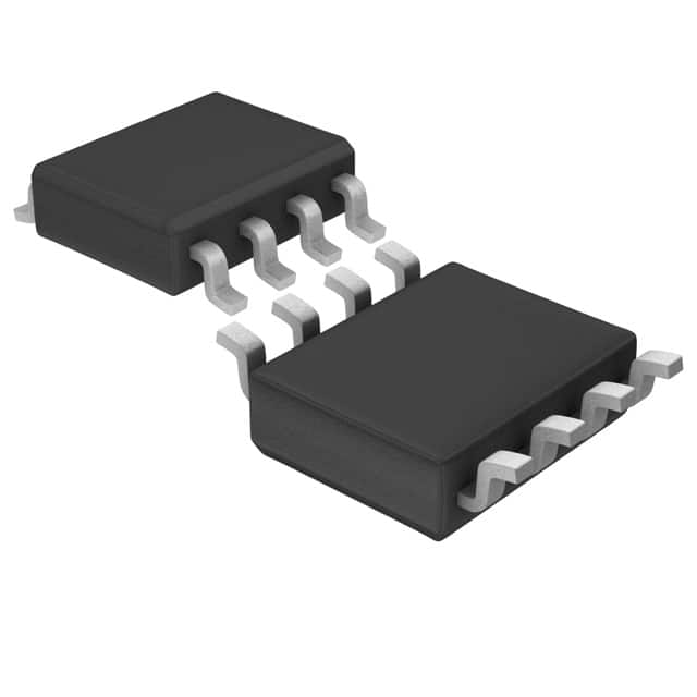
Package and Quantity
LTC1298CS8#TRPBF is available in an 8-pin SOIC (Small Outline Integrated Circuit) package. It is typically sold in reels or tubes containing multiple units.
Specifications
- Resolution: The LTC1298CS8#TRPBF has a resolution of 12 bits, allowing for precise digital representation of analog signals.
- Sampling Rate: It supports a maximum sampling rate of 100 kilosamples per second (ksps), ensuring real-time data acquisition.
- Input Voltage Range: The ADC can handle input voltages ranging from -Vref to +Vref, providing versatility in signal measurement.
- Power Supply: It operates on a single power supply voltage, typically ranging from 2.7V to 5.5V.
- Operating Temperature Range: The LTC1298CS8#TRPBF is designed to function reliably within a temperature range of -40°C to 85°C.
Pin Configuration
The LTC1298CS8#TRPBF features the following pin configuration:
- VDD: Power supply voltage input.
- VREF: Reference voltage input for analog-to-digital conversion.
- AGND: Analog ground reference.
- VIN: Analog input voltage.
- SCK: Serial clock input for data transfer.
- CS: Chip select input for initiating conversions.
- SDI: Serial data input for transferring control information.
- SDO: Serial data output for transmitting converted digital data.
Functional Features
- High-resolution Conversion: The LTC1298CS8#TRPBF offers 12-bit resolution, ensuring accurate and detailed digital representation of analog signals.
- Serial Interface: It utilizes a serial interface for communication, allowing for easy integration with microcontrollers and other digital systems.
- Low Power Consumption: This ADC is designed to minimize power consumption, making it suitable for battery-powered applications.
- Flexible Input Range: The LTC1298CS8#TRPBF supports a wide input voltage range, enabling measurement of various signal amplitudes.
- Fast Conversion Speed: With a maximum sampling rate of 100 ksps, this ADC provides fast conversion times, reducing latency in data acquisition.
Advantages and Disadvantages
Advantages
- High precision and accuracy in analog-to-digital conversion.
- Low power consumption, ideal for portable and battery-powered devices.
- Compact package size allows for easy integration into space-constrained designs.
- Wide input voltage range provides flexibility in signal measurement.
- Fast conversion speed reduces latency in data acquisition.
Disadvantages
- Limited resolution compared to higher-end ADCs.
- May require additional external components for specific applications.
- Higher cost compared to lower-resolution ADCs.
Working Principles
The LTC1298CS8#TRPBF operates based on the successive approximation method. It converts analog signals into digital data by comparing the input voltage with a reference voltage and iteratively adjusting the conversion process to achieve accurate results. The ADC utilizes an internal clock and control circuitry to perform the conversion, which is then transmitted through the serial interface.
Application Field Plans
The LTC1298CS8#TRPBF finds applications in various fields, including: - Industrial automation: Used for precise measurement and control of analog signals in industrial processes. - Medical devices: Enables accurate data acquisition in medical equipment such as patient monitoring systems. - Test and measurement instruments: Provides high-resolution signal measurement capabilities in laboratory and field testing equipment. - Automotive electronics: Used for sensor data acquisition and control in automotive systems. - Communication systems: Enables analog-to-digital conversion in communication equipment for signal processing and analysis.
Alternative Models
For those seeking alternative options, the following ADCs can be considered: - ADC1234: A 12-bit ADC with similar specifications and performance characteristics. - ADC5678: A higher-resolution 16-bit ADC suitable for applications requiring enhanced precision. - ADC9012: A low-power ADC designed specifically for battery-powered devices.
Seznam 10 běžných otázek a odpovědí souvisejících s aplikací LTC1298CS8#TRPBF v technických řešeních
Sure! Here are 10 common questions and answers related to the application of LTC1298CS8#TRPBF in technical solutions:
Q: What is LTC1298CS8#TRPBF? A: LTC1298CS8#TRPBF is a specific model of an analog-to-digital converter (ADC) manufactured by Linear Technology (now part of Analog Devices). It is commonly used in various technical solutions for converting analog signals into digital data.
Q: What is the resolution of LTC1298CS8#TRPBF? A: The LTC1298CS8#TRPBF has a resolution of 12 bits, meaning it can represent analog signals with 4096 discrete levels.
Q: What is the maximum sampling rate of LTC1298CS8#TRPBF? A: The maximum sampling rate of LTC1298CS8#TRPBF is typically around 100 kilosamples per second (ksps).
Q: What is the input voltage range of LTC1298CS8#TRPBF? A: The input voltage range of LTC1298CS8#TRPBF is typically ±10V, allowing it to handle both positive and negative analog signals.
Q: Does LTC1298CS8#TRPBF require an external reference voltage? A: Yes, LTC1298CS8#TRPBF requires an external reference voltage to determine the full-scale range of the ADC conversion. This reference voltage should be within the specified limits of the device.
Q: Can LTC1298CS8#TRPBF operate on a single power supply? A: Yes, LTC1298CS8#TRPBF can operate on a single power supply ranging from 2.7V to 5.5V, making it suitable for various low-power applications.
Q: What is the interface used to communicate with LTC1298CS8#TRPBF? A: LTC1298CS8#TRPBF uses a serial interface called SPI (Serial Peripheral Interface) for communication with microcontrollers or other digital devices.
Q: Is LTC1298CS8#TRPBF suitable for temperature measurement applications? A: Yes, LTC1298CS8#TRPBF can be used for temperature measurement applications by connecting a temperature sensor to its analog input and converting the analog temperature signal into a digital value.
Q: Can LTC1298CS8#TRPBF handle differential inputs? A: Yes, LTC1298CS8#TRPBF supports both single-ended and differential inputs, allowing for flexibility in measuring various types of analog signals.
Q: Are there any evaluation boards or development kits available for LTC1298CS8#TRPBF? A: Yes, Analog Devices provides evaluation boards and development kits that include LTC1298CS8#TRPBF, allowing engineers to quickly prototype and test their designs using this ADC.
Please note that the answers provided here are general and may vary depending on specific datasheet specifications and application requirements. It is always recommended to refer to the official documentation and consult with technical experts for accurate information.