

Viz Specifikace pro podrobnosti o produktu.
LTC1323CS16#TRPBF
Product Overview
Category
LTC1323CS16#TRPBF belongs to the category of integrated circuits (ICs).
Use
This product is commonly used in electronic devices for signal conditioning and data acquisition applications.
Characteristics
- LTC1323CS16#TRPBF is a low-power, 12-bit analog-to-digital converter (ADC) with a maximum sampling rate of 100 kilosamples per second (ksps).
- It operates on a single 5V power supply and features a differential input voltage range of ±10V.
- The ADC utilizes a successive approximation register (SAR) architecture, providing accurate conversion results.
- It offers a high signal-to-noise ratio (SNR) and low total harmonic distortion (THD), ensuring reliable and precise measurements.
- The device incorporates an internal reference voltage and temperature sensor, enhancing its performance and versatility.
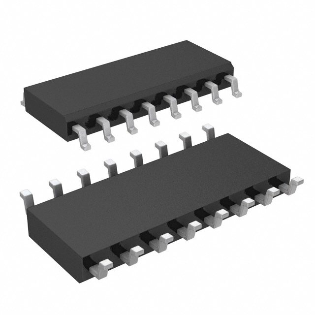
- LTC1323CS16#TRPBF is available in a small 16-pin surface mount package, making it suitable for space-constrained applications.
Packaging/Quantity
The LTC1323CS16#TRPBF is typically packaged in tape and reel format, with 250 units per reel.
Specifications
- Resolution: 12 bits
- Sampling Rate: Up to 100 ksps
- Power Supply: 5V
- Input Voltage Range: ±10V
- Reference Voltage: Internal
- Temperature Sensor: Built-in
- Package Type: 16-pin surface mount
Detailed Pin Configuration
- VDD - Power supply voltage
- AGND - Analog ground
- REF - Reference voltage output
- IN+ - Positive differential input
- IN- - Negative differential input
- CS - Chip select input
- SCK - Serial clock input
- SDI - Serial data input
- SDO - Serial data output
- SDO/EOC - Serial data output/End of conversion
- DGND - Digital ground
- CLKOUT - Clock output
- VREF - Reference voltage input
- TEMP - Temperature sensor output
- NC - No connection
- VSS - Ground
Functional Features
- High-resolution ADC with 12-bit accuracy
- Low-power consumption for energy-efficient operation
- Fast sampling rate of up to 100 ksps
- Differential input configuration for improved noise rejection
- Internal reference voltage and temperature sensor for enhanced performance
- Serial interface for easy integration with microcontrollers or other digital devices
Advantages and Disadvantages
Advantages
- High accuracy and resolution for precise measurements
- Low power consumption for energy efficiency
- Compact package size suitable for space-constrained applications
- Built-in reference voltage and temperature sensor reduce external component requirements
- Fast sampling rate enables real-time data acquisition
Disadvantages
- Limited input voltage range compared to some other ADCs
- Requires an external clock source for proper operation
- Higher cost compared to lower-resolution ADCs
Working Principles
The LTC1323CS16#TRPBF operates based on the successive approximation register (SAR) architecture. It converts analog signals into digital data by comparing the input voltage with a series of binary-weighted voltages generated internally. The SAR algorithm successively approximates the input voltage until the digital representation is obtained.
The device utilizes a differential input configuration, which improves noise rejection and common-mode rejection ratio (CMRR). This ensures accurate and reliable conversion results even in noisy environments.
The built-in reference voltage and temperature sensor contribute to the overall performance of the ADC. The internal reference voltage provides a stable and accurate voltage reference for the conversion process. Additionally, the temperature sensor output allows compensation for variations in the ADC's performance due to temperature changes.
Detailed Application Field Plans
The LTC1323CS16#TRPBF finds applications in various fields, including:
- Industrial Automation: Used for data acquisition and control systems in industrial processes.
- Medical Devices: Enables accurate measurement and monitoring of vital signs and patient parameters.
- Test and Measurement Equipment: Provides high-resolution measurements for scientific and engineering instruments.
- Communication Systems: Used in signal processing and modulation/demodulation applications.
- Automotive Electronics: Enables precise sensing and control in automotive systems.
Detailed and Complete Alternative Models
- LTC1323CS8#TRPBF: Similar to LTC1323CS16#TRPBF but with an 8-pin surface mount package.
- LTC1323IS8#TRPBF: Improved version with higher sampling rate and lower power consumption.
- LTC1323CS16-12#TRPBF: Lower resolution variant with 12-bit accuracy.
These alternative models offer similar functionality and characteristics, allowing users to choose the most suitable option based on their specific requirements.
*
Seznam 10 běžných otázek a odpovědí souvisejících s aplikací LTC1323CS16#TRPBF v technických řešeních
Sure! Here are 10 common questions and answers related to the application of LTC1323CS16#TRPBF in technical solutions:
Q: What is LTC1323CS16#TRPBF? A: LTC1323CS16#TRPBF is a specific model number for a digital-to-analog converter (DAC) chip manufactured by Linear Technology (now part of Analog Devices).
Q: What is the purpose of LTC1323CS16#TRPBF? A: The LTC1323CS16#TRPBF DAC chip is used to convert digital signals into analog voltages, making it suitable for various applications such as audio systems, instrumentation, and control systems.
Q: What is the operating voltage range of LTC1323CS16#TRPBF? A: The LTC1323CS16#TRPBF operates within a voltage range of 2.7V to 5.5V.
Q: How many bits does LTC1323CS16#TRPBF support? A: LTC1323CS16#TRPBF is a 12-bit DAC, meaning it can convert digital inputs into analog outputs with a resolution of up to 4096 levels.
Q: What is the output voltage range of LTC1323CS16#TRPBF? A: The output voltage range of LTC1323CS16#TRPBF is typically between 0V and Vref, where Vref is the reference voltage supplied to the chip.
Q: Can LTC1323CS16#TRPBF be used in both single-ended and differential output configurations? A: Yes, LTC1323CS16#TRPBF supports both single-ended and differential output configurations, providing flexibility in different system designs.
Q: What is the maximum settling time of LTC1323CS16#TRPBF? A: The maximum settling time of LTC1323CS16#TRPBF is typically around 10µs, ensuring fast and accurate conversion.
Q: Does LTC1323CS16#TRPBF have built-in power-on reset circuitry? A: Yes, LTC1323CS16#TRPBF includes a power-on reset circuit that ensures the DAC output initializes to zero volts upon power-up.
Q: Can LTC1323CS16#TRPBF operate in both single-supply and dual-supply configurations? A: Yes, LTC1323CS16#TRPBF can be operated with either a single positive supply or a dual positive/negative supply, depending on the system requirements.
Q: Is LTC1323CS16#TRPBF available in different package options? A: Yes, LTC1323CS16#TRPBF is available in a 16-pin narrow SOIC (Small Outline Integrated Circuit) package, which is commonly used in many electronic systems.
Please note that the answers provided here are general and may vary based on specific datasheet information and application requirements.