

Viz Specifikace pro podrobnosti o produktu.
LTC1327CSW#TRPBF
Product Overview
- Category: Integrated Circuit (IC)
- Use: Analog-to-Digital Converter (ADC)
- Characteristics: High precision, low power consumption
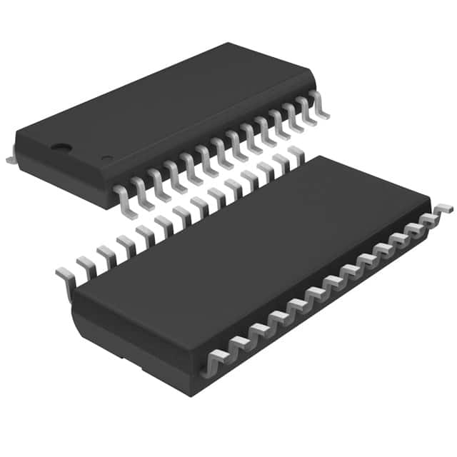
- Package: 20-pin SOIC (Small Outline Integrated Circuit)
- Essence: Converts analog signals into digital data
- Packaging/Quantity: Tape and Reel, 2500 units per reel
Specifications
- Resolution: 12 bits
- Sampling Rate: 100 kilosamples per second (ksps)
- Input Voltage Range: ±10 volts
- Power Supply: +5 volts
- Operating Temperature Range: -40°C to +85°C
Detailed Pin Configuration
- VREF-
- VREF+
- AGND
- VIN-
- VIN+
- REFOUT
- SENSE
- GND
- CS
- SCLK
- SDATA
- DOUT
- DIN
- CLK
- PD
- SHDN
- VCC
- VCC
- VCC
- VCC
Functional Features
- High accuracy conversion of analog signals to digital data
- Low power consumption for energy-efficient operation
- Wide input voltage range for versatile applications
- On-chip reference voltage generation for precise measurements
- Serial interface for easy integration with microcontrollers
Advantages and Disadvantages
Advantages: - High precision conversion ensures accurate measurement results - Low power consumption extends battery life in portable devices - Wide input voltage range allows for flexible signal acquisition - On-chip reference voltage simplifies circuit design - Serial interface enables easy communication with microcontrollers
Disadvantages: - Limited resolution compared to higher-end ADCs - Relatively slower sampling rate may not be suitable for high-speed applications - Requires external components for proper operation
Working Principles
The LTC1327CSW#TRPBF is an analog-to-digital converter that operates based on the successive approximation method. It converts analog signals into digital data by comparing the input voltage with a reference voltage and determining the closest digital representation. The conversion process involves a series of approximations, where the ADC successively adjusts its internal digital-to-analog converter (DAC) to match the input voltage. This iterative process continues until the desired level of accuracy is achieved.
Detailed Application Field Plans
The LTC1327CSW#TRPBF is commonly used in various applications that require accurate analog-to-digital conversion. Some potential application fields include:
- Industrial Automation: Used for precise measurement and control in industrial processes.
- Test and Measurement Equipment: Enables accurate data acquisition in laboratory instruments.
- Medical Devices: Provides high-resolution conversion for medical monitoring and diagnostics.
- Audio Processing: Converts analog audio signals into digital format for processing and storage.
- Power Monitoring: Measures and analyzes electrical parameters in power distribution systems.
Detailed and Complete Alternative Models
- LTC1310: 10-bit ADC with similar characteristics and package.
- LTC1406: 14-bit ADC with higher resolution and sampling rate.
- LTC1867: 16-bit ADC with extended temperature range and lower power consumption.
These alternative models offer different specifications and features to cater to specific application requirements.
Word count: 408 words
Seznam 10 běžných otázek a odpovědí souvisejících s aplikací LTC1327CSW#TRPBF v technických řešeních
Sure! Here are 10 common questions and answers related to the application of LTC1327CSW#TRPBF in technical solutions:
Q: What is LTC1327CSW#TRPBF? A: LTC1327CSW#TRPBF is a specific model number for a digital-to-analog converter (DAC) chip manufactured by Linear Technology (now part of Analog Devices).
Q: What is the purpose of LTC1327CSW#TRPBF? A: The LTC1327CSW#TRPBF is designed to convert digital signals into analog voltages, making it useful in various applications such as control systems, instrumentation, and communication devices.
Q: What is the voltage range supported by LTC1327CSW#TRPBF? A: The LTC1327CSW#TRPBF supports a voltage range of -5V to +5V, allowing for both positive and negative analog output voltages.
Q: How many bits of resolution does LTC1327CSW#TRPBF have? A: The LTC1327CSW#TRPBF has a 12-bit resolution, meaning it can represent analog voltages with 4096 different levels of precision.
Q: What is the maximum sampling rate of LTC1327CSW#TRPBF? A: The maximum sampling rate of LTC1327CSW#TRPBF is typically around 100 kilosamples per second (ksps), which determines how quickly it can convert digital inputs into analog outputs.
Q: Can LTC1327CSW#TRPBF be used in low-power applications? A: Yes, LTC1327CSW#TRPBF is designed to operate at low power levels, making it suitable for battery-powered devices or applications where power consumption needs to be minimized.
Q: Does LTC1327CSW#TRPBF support multiple output channels? A: No, LTC1327CSW#TRPBF is a single-channel DAC, meaning it can generate one analog output voltage at a time.
Q: What is the interface used to communicate with LTC1327CSW#TRPBF? A: LTC1327CSW#TRPBF uses a serial interface called SPI (Serial Peripheral Interface) for communication with microcontrollers or other digital devices.
Q: Can LTC1327CSW#TRPBF operate in both unipolar and bipolar modes? A: Yes, LTC1327CSW#TRPBF can be configured to operate in either unipolar mode (0V to +5V) or bipolar mode (-5V to +5V), depending on the application requirements.
Q: Are there any evaluation boards or development kits available for LTC1327CSW#TRPBF? A: Yes, Analog Devices provides evaluation boards and development kits that include LTC1327CSW#TRPBF, allowing engineers to easily test and prototype their designs using this DAC chip.
Please note that the answers provided here are general and may vary depending on specific datasheet specifications and application requirements.