

Viz Specifikace pro podrobnosti o produktu.
LTC1542CDD#TRPBF
Product Overview
Category
LTC1542CDD#TRPBF belongs to the category of integrated circuits (ICs).
Use
This IC is commonly used in electronic devices for signal switching and amplification.
Characteristics
- Low power consumption
- High-speed operation
- Wide operating voltage range
- Small package size
- RoHS compliant
Package
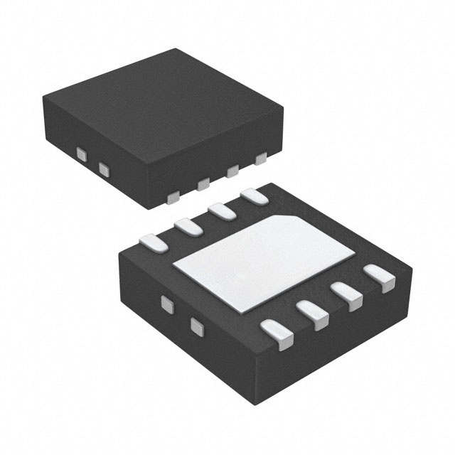
LTC1542CDD#TRPBF is available in a DFN-8 (Dual Flat No-Lead) package.
Essence
The essence of LTC1542CDD#TRPBF lies in its ability to efficiently switch and amplify signals while consuming minimal power.
Packaging/Quantity
This IC is typically packaged in reels, with each reel containing 2500 units.
Specifications
- Supply Voltage: 2.7V to 5.5V
- Operating Temperature Range: -40°C to 85°C
- Input Voltage Range: 0V to Vcc
- Output Voltage Range: 0V to Vcc
- Quiescent Current: 1.5μA (typical)
- Bandwidth: 10MHz (typical)
Detailed Pin Configuration
LTC1542CDD#TRPBF has the following pin configuration:
```
| | --| IN1 |-- --| IN2 |-- --| OUT |-- --| GND |-- --| EN |-- --| Vcc |-- --|___________|-- ```
Functional Features
- Dual input channels for signal selection
- Single output channel for amplified signal
- Enable pin for controlling the IC's operation
- Low quiescent current for power efficiency
- Wide operating voltage range for versatility
Advantages and Disadvantages
Advantages
- Low power consumption extends battery life in portable devices.
- High-speed operation allows for efficient signal processing.
- Wide operating voltage range enables compatibility with various power sources.
- Small package size saves valuable board space.
- RoHS compliance ensures environmental friendliness.
Disadvantages
- Limited number of input channels may restrict certain applications.
- May require additional external components for specific circuit configurations.
Working Principles
LTC1542CDD#TRPBF operates by selectively routing the input signals from IN1 or IN2 to the output channel. The enable pin (EN) controls the IC's operation, allowing the user to activate or deactivate the signal switching functionality. When enabled, the IC amplifies the selected input signal and routes it to the output pin (OUT). The low quiescent current ensures minimal power consumption during operation.
Detailed Application Field Plans
LTC1542CDD#TRPBF finds applications in various fields, including:
- Audio Systems: Signal selection and amplification in audio mixers and receivers.
- Communication Devices: Switching between different communication channels in radios and telecommunication equipment.
- Test and Measurement Instruments: Signal routing and amplification in oscilloscopes and data acquisition systems.
- Industrial Automation: Control signal selection and amplification in PLCs (Programmable Logic Controllers) and industrial control systems.
Detailed and Complete Alternative Models
- LTC1542CMS8#PBF: Similar specifications and features, but available in an MSOP-8 package.
- MAX4617ESE+: Comparable performance with additional ESD protection, available in an SOIC-16 package.
- ADG1419BRMZ: Higher bandwidth and lower on-resistance, available in a 10-lead MSOP package.
These alternative models offer similar functionality and can be considered as substitutes for LTC1542CDD#TRPBF in various applications.
Word count: 513 words
Seznam 10 běžných otázek a odpovědí souvisejících s aplikací LTC1542CDD#TRPBF v technických řešeních
Sure! Here are 10 common questions and answers related to the application of LTC1542CDD#TRPBF in technical solutions:
Q: What is LTC1542CDD#TRPBF? A: LTC1542CDD#TRPBF is a specific model number for a low-power, dual comparator IC (integrated circuit) manufactured by Linear Technology.
Q: What are the key features of LTC1542CDD#TRPBF? A: Some key features of LTC1542CDD#TRPBF include low supply current, wide input voltage range, rail-to-rail outputs, and low propagation delay.
Q: What are the typical applications of LTC1542CDD#TRPBF? A: LTC1542CDD#TRPBF is commonly used in battery-powered systems, portable devices, power management circuits, and general-purpose comparator applications.
Q: What is the supply voltage range for LTC1542CDD#TRPBF? A: The supply voltage range for LTC1542CDD#TRPBF is typically between 2.7V and 11V.
Q: Can LTC1542CDD#TRPBF operate with a single power supply? A: Yes, LTC1542CDD#TRPBF can operate with a single power supply as it has rail-to-rail outputs.
Q: What is the maximum output current of LTC1542CDD#TRPBF? A: The maximum output current of LTC1542CDD#TRPBF is typically around 20mA.
Q: Does LTC1542CDD#TRPBF have built-in hysteresis? A: No, LTC1542CDD#TRPBF does not have built-in hysteresis. External components may be required to add hysteresis if needed.
Q: What is the operating temperature range for LTC1542CDD#TRPBF? A: The operating temperature range for LTC1542CDD#TRPBF is typically between -40°C and 85°C.
Q: Can LTC1542CDD#TRPBF tolerate overvoltage conditions? A: Yes, LTC1542CDD#TRPBF has built-in ESD (electrostatic discharge) protection, which helps it tolerate overvoltage conditions.
Q: Is there a recommended evaluation board or reference design available for LTC1542CDD#TRPBF? A: Yes, Linear Technology provides an evaluation board called DC1010A for LTC1542CDD#TRPBF, which can be used for testing and prototyping purposes.
Please note that the answers provided here are general and may vary depending on the specific datasheet and application requirements. It's always recommended to refer to the official documentation and consult with technical experts for accurate information.