

Viz Specifikace pro podrobnosti o produktu.
LTC1597-1BCG#PBF
Product Overview
Category: Integrated Circuit (IC)
Use: Digital-to-Analog Converter (DAC)
Characteristics: - High-resolution DAC with 16-bit accuracy - Low power consumption - Fast settling time - Wide operating voltage range - Small package size
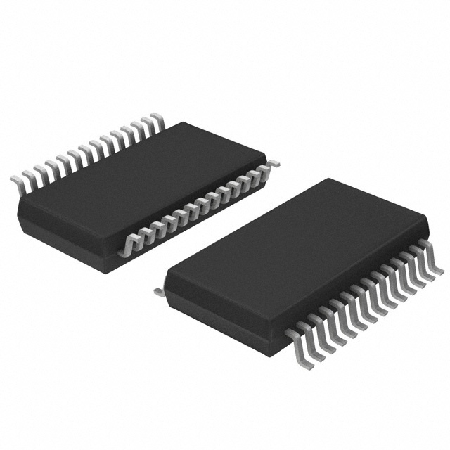
Package: Ceramic Grid Array (CGA)
Essence: The LTC1597-1BCG#PBF is a high-performance DAC designed for various applications requiring precise analog output.
Packaging/Quantity: The LTC1597-1BCG#PBF is available in tape and reel packaging, with a quantity of 250 units per reel.
Specifications
- Resolution: 16 bits
- Supply Voltage Range: 2.7V to 5.5V
- Output Voltage Range: 0V to Vref
- Integral Nonlinearity (INL): ±1 LSB (max)
- Differential Nonlinearity (DNL): ±0.5 LSB (max)
- Settling Time: 4µs (typ)
- Operating Temperature Range: -40°C to +85°C
Pin Configuration
The LTC1597-1BCG#PBF has a total of 20 pins. The pin configuration is as follows:
Pin 1: VDD
Pin 2: GND
Pin 3: REF
Pin 4: AGND
Pin 5: AOUT
Pin 6: DB15
Pin 7: DB14
Pin 8: DB13
Pin 9: DB12
Pin 10: DB11
Pin 11: DB10
Pin 12: DB9
Pin 13: DB8
Pin 14: DB7
Pin 15: DB6
Pin 16: DB5
Pin 17: DB4
Pin 18: DB3
Pin 19: DB2
Pin 20: DB1
Functional Features
- High-resolution digital-to-analog conversion
- Low power consumption for energy-efficient operation
- Fast settling time ensures quick response
- Wide operating voltage range allows flexibility in various applications
- Small package size enables space-saving designs
Advantages and Disadvantages
Advantages: - High accuracy with 16-bit resolution - Low power consumption for energy efficiency - Fast settling time for quick response - Wide operating voltage range for versatility - Compact package size for space-saving designs
Disadvantages: - Limited output voltage range (0V to Vref) - Relatively high cost compared to lower-resolution DACs
Working Principles
The LTC1597-1BCG#PBF operates by converting digital input signals into precise analog output voltages. It utilizes a 16-bit resolution to achieve high accuracy in the conversion process. The internal circuitry ensures low power consumption while maintaining fast settling time for efficient performance.
Detailed Application Field Plans
The LTC1597-1BCG#PBF finds applications in various fields where accurate analog output is required. Some potential application areas include: - Audio equipment - Instrumentation and measurement devices - Industrial control systems - Communication systems - Test and measurement equipment
Detailed and Complete Alternative Models
- LTC1596-1BCG#PBF: 16-bit DAC with similar characteristics and pin configuration
- LTC1598-1BCG#PBF: 16-bit DAC with extended temperature range
- LTC1597-2BCG#PBF: 16-bit dual-channel DAC with similar characteristics and pin configuration
These alternative models offer similar functionality and can be considered as substitutes for the LTC1597-1BCG#PBF in specific applications.
Word count: 346 words
Seznam 10 běžných otázek a odpovědí souvisejících s aplikací LTC1597-1BCG#PBF v technických řešeních
Sure! Here are 10 common questions and answers related to the application of LTC1597-1BCG#PBF in technical solutions:
Q1: What is LTC1597-1BCG#PBF? A1: LTC1597-1BCG#PBF is a specific model number for a digital-to-analog converter (DAC) manufactured by Linear Technology Corporation.
Q2: What is the purpose of LTC1597-1BCG#PBF? A2: The LTC1597-1BCG#PBF is designed to convert digital signals into analog voltages, making it useful in various applications such as audio systems, instrumentation, and control systems.
Q3: What is the resolution of LTC1597-1BCG#PBF? A3: The LTC1597-1BCG#PBF has a resolution of 12 bits, meaning it can represent analog voltages with 4096 discrete levels.
Q4: What is the operating voltage range of LTC1597-1BCG#PBF? A4: The LTC1597-1BCG#PBF operates from a single power supply voltage ranging from 2.7V to 5.5V.
Q5: What is the output voltage range of LTC1597-1BCG#PBF? A5: The output voltage range of LTC1597-1BCG#PBF is programmable and can be set between 0V and the reference voltage applied to the device.
Q6: How does LTC1597-1BCG#PBF communicate with a microcontroller or other digital devices? A6: LTC1597-1BCG#PBF uses a serial interface called SPI (Serial Peripheral Interface) to communicate with external devices.
Q7: Can LTC1597-1BCG#PBF be used in both single-ended and differential output configurations? A7: Yes, LTC1597-1BCG#PBF can be configured for both single-ended and differential output modes, providing flexibility in various applications.
Q8: What is the settling time of LTC1597-1BCG#PBF? A8: The settling time of LTC1597-1BCG#PBF is typically 4.5μs, which refers to the time it takes for the output voltage to reach within a specified error band after a change in the digital input.
Q9: Does LTC1597-1BCG#PBF have any built-in reference voltage? A9: No, LTC1597-1BCG#PBF requires an external reference voltage to determine its output range.
Q10: Is LTC1597-1BCG#PBF available in different package options? A10: Yes, LTC1597-1BCG#PBF is available in various package options, including the 16-pin SSOP (Shrink Small Outline Package) and the 16-pin DFN (Dual Flat No-Lead) package.
Please note that the answers provided here are general and may vary depending on the specific datasheet and application requirements.