

Viz Specifikace pro podrobnosti o produktu.
LTC1663-2CS5#TRMPBF
Product Overview
Category
The LTC1663-2CS5#TRMPBF belongs to the category of digital-to-analog converters (DACs).
Use
This product is commonly used in various electronic devices and systems where analog signals need to be converted into digital form for processing or control purposes.
Characteristics
- High precision: The LTC1663-2CS5#TRMPBF offers high-resolution conversion, ensuring accurate representation of analog signals.
- Low power consumption: This DAC operates with low power requirements, making it suitable for battery-powered applications.
- Small package size: The LTC1663-2CS5#TRMPBF is available in a compact CS5 package, enabling space-efficient integration into electronic designs.
- Wide voltage range: It supports a wide supply voltage range, allowing compatibility with different power sources.
- Fast conversion speed: This DAC provides fast conversion times, facilitating real-time signal processing.
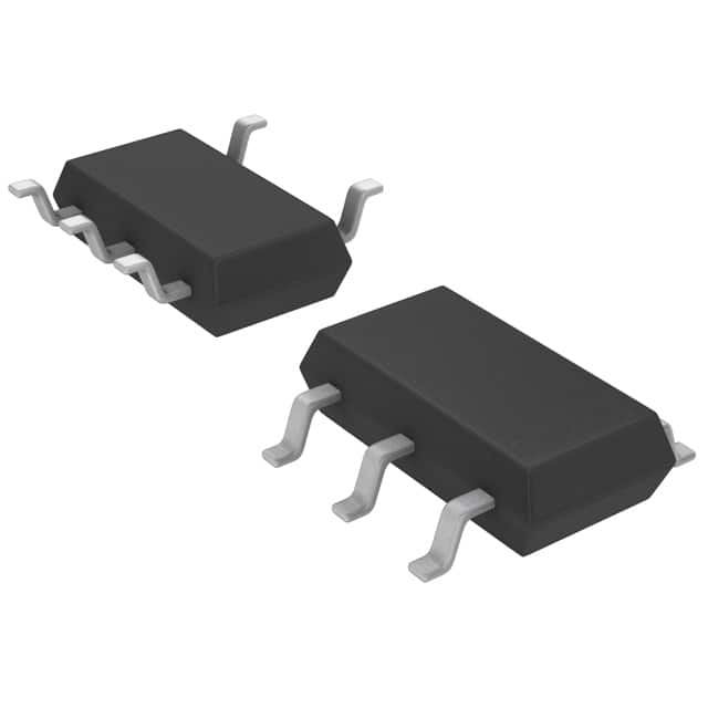
Package and Quantity
The LTC1663-2CS5#TRMPBF is packaged in a CS5 package. Each package contains one unit of the LTC1663-2CS5#TRMPBF DAC.
Specifications
- Resolution: 16 bits
- Supply Voltage Range: 2.7V to 5.5V
- Conversion Speed: Up to 1Msps
- Operating Temperature Range: -40°C to 85°C
- Interface: Serial SPI/I2C
- Output Type: Voltage
Pin Configuration
The LTC1663-2CS5#TRMPBF follows the standard pin configuration for digital-to-analog converters. The pinout is as follows:
- VDD: Power supply voltage
- GND: Ground reference
- SDA/SCL: Serial data input/output or serial clock input (depending on the interface mode)
- CS: Chip select input
- REF: Reference voltage input
- AGND: Analog ground reference
- OUT: Analog output voltage
Functional Features
- High-resolution conversion: The LTC1663-2CS5#TRMPBF provides 16-bit resolution, ensuring accurate representation of analog signals.
- Flexible interface options: It supports both SPI and I2C interfaces, allowing compatibility with various microcontrollers and digital systems.
- Low power consumption: This DAC operates with low power requirements, making it suitable for energy-efficient applications.
- Output voltage range control: The LTC1663-2CS5#TRMPBF allows users to adjust the output voltage range according to their specific needs.
- Digital gain adjustment: It offers digital gain control, enabling fine-tuning of the output signal amplitude.
Advantages and Disadvantages
Advantages
- High precision and accuracy in analog-to-digital conversion.
- Compact package size for space-constrained designs.
- Wide supply voltage range for versatile power source compatibility.
- Fast conversion speed for real-time signal processing.
Disadvantages
- Limited output current capability.
- Requires an external reference voltage source for operation.
Working Principles
The LTC1663-2CS5#TRMPBF operates based on the principle of digital-to-analog conversion. It receives digital input data through the selected interface (SPI or I2C) and converts it into a corresponding analog voltage output. The resolution of 16 bits ensures precise representation of the digital input values in the analog domain. The output voltage can be adjusted using the provided control features, such as gain control and voltage range selection.
Application Field Plans
The LTC1663-2CS5#TRMPBF finds application in various fields, including:
- Audio equipment: It can be used in audio amplifiers, mixers, and digital audio workstations to convert digital audio signals into analog form for amplification and playback.
- Industrial automation: This DAC is suitable for control systems that require precise analog voltage generation, such as motor control, robotics, and process control.
- Test and measurement instruments: It can be integrated into oscilloscopes, data loggers, and signal generators to provide accurate analog output signals for testing and calibration purposes.
- Communication systems: The LTC1663-2CS5#TRMPBF can be utilized in wireless communication devices, base stations, and transceivers for generating analog signals used in modulation and demodulation processes.
Alternative Models
- MAX5216: 16-bit DAC with similar features and performance characteristics.
- AD5668: 16-bit DAC offering a different package option and interface compatibility.
- MCP4922: 12-bit DAC with lower resolution but suitable for cost-sensitive applications.
These alternative models can be considered based on specific design requirements and preferences.
Word count: 550 words
Seznam 10 běžných otázek a odpovědí souvisejících s aplikací LTC1663-2CS5#TRMPBF v technických řešeních
Sure! Here are 10 common questions and answers related to the application of LTC1663-2CS5#TRMPBF in technical solutions:
Q: What is LTC1663-2CS5#TRMPBF? A: LTC1663-2CS5#TRMPBF is a specific model of digital-to-analog converter (DAC) manufactured by Linear Technology (now part of Analog Devices). It is designed for precision voltage output applications.
Q: What is the operating voltage range of LTC1663-2CS5#TRMPBF? A: The operating voltage range of LTC1663-2CS5#TRMPBF is typically between 2.7V and 5.5V.
Q: How many bits of resolution does LTC1663-2CS5#TRMPBF have? A: LTC1663-2CS5#TRMPBF has 16 bits of resolution, allowing for high precision analog output.
Q: What is the maximum output voltage range of LTC1663-2CS5#TRMPBF? A: The maximum output voltage range of LTC1663-2CS5#TRMPBF is typically between 0V and VREF, where VREF is the reference voltage supplied to the DAC.
Q: Can LTC1663-2CS5#TRMPBF be used in both single-ended and differential output configurations? A: Yes, LTC1663-2CS5#TRMPBF can be used in both single-ended and differential output configurations, providing flexibility in various applications.
Q: What is the typical settling time of LTC1663-2CS5#TRMPBF? A: The typical settling time of LTC1663-2CS5#TRMPBF is around 10µs, ensuring fast and accurate voltage output.
Q: Does LTC1663-2CS5#TRMPBF have an integrated reference voltage source? A: No, LTC1663-2CS5#TRMPBF does not have an integrated reference voltage source. An external reference voltage must be provided to the DAC.
Q: Can LTC1663-2CS5#TRMPBF operate in both single-supply and dual-supply configurations? A: Yes, LTC1663-2CS5#TRMPBF can operate in both single-supply and dual-supply configurations, making it suitable for a wide range of applications.
Q: What is the power supply current requirement of LTC1663-2CS5#TRMPBF? A: The power supply current requirement of LTC1663-2CS5#TRMPBF is typically around 1.5mA, which may vary depending on the operating conditions.
Q: Is LTC1663-2CS5#TRMPBF available in a surface-mount package? A: Yes, LTC1663-2CS5#TRMPBF is available in a surface-mount package with the part number CS5, making it suitable for compact and space-constrained designs.
Please note that the answers provided here are general and may vary based on specific datasheet specifications and application requirements.