

Viz Specifikace pro podrobnosti o produktu.
LTC2629IGN#TRPBF
Product Overview
- Category: Integrated Circuit (IC)
- Use: Digital-to-Analog Converter (DAC)
- Characteristics: High precision, low power consumption
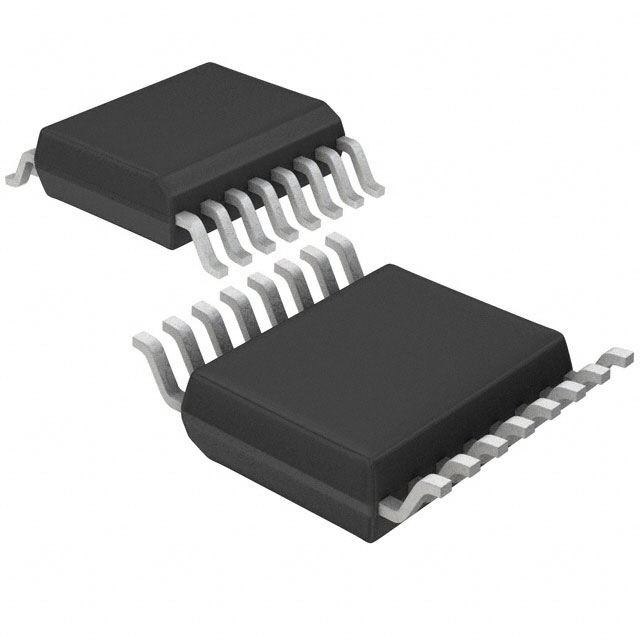
- Package: 16-Lead SSOP
- Essence: Converts digital signals into analog voltages
- Packaging/Quantity: Tape & Reel, 2500 units per reel
Specifications
- Resolution: 12 bits
- Number of Channels: 8
- Interface: I2C
- Supply Voltage: 2.7V to 5.5V
- Operating Temperature Range: -40°C to +85°C
Detailed Pin Configuration
The LTC2629IGN#TRPBF has a total of 16 pins. The pin configuration is as follows:
- VDD - Power supply voltage
- SDA - Serial data input
- SCL - Serial clock input
- A0 - Address input bit 0
- A1 - Address input bit 1
- A2 - Address input bit 2
- REF - Reference voltage input
- GND - Ground
- DAC0 - Analog output channel 0
- DAC1 - Analog output channel 1
- DAC2 - Analog output channel 2
- DAC3 - Analog output channel 3
- DAC4 - Analog output channel 4
- DAC5 - Analog output channel 5
- DAC6 - Analog output channel 6
- DAC7 - Analog output channel 7
Functional Features
- High accuracy and resolution for precise analog voltage generation
- Low power consumption for energy-efficient applications
- I2C interface allows easy communication with microcontrollers or other digital devices
- Internal reference voltage simplifies system design
- Output voltage range can be programmed to suit specific requirements
Advantages and Disadvantages
Advantages: - High precision and resolution - Low power consumption - Easy integration with digital systems - Flexible output voltage range programming
Disadvantages: - Limited number of channels (8) - Requires external reference voltage for accurate analog output
Working Principles
The LTC2629IGN#TRPBF is a digital-to-analog converter (DAC) that converts digital signals into corresponding analog voltages. It utilizes an internal reference voltage and an I2C interface to receive digital input data and generate precise analog outputs. The device operates within a specified supply voltage range and can be controlled by a microcontroller or other digital devices.
Detailed Application Field Plans
The LTC2629IGN#TRPBF is commonly used in various applications that require accurate analog voltage generation. Some potential application fields include:
- Industrial Automation: Control systems, process monitoring, and instrumentation.
- Test and Measurement Equipment: Signal generation, calibration, and data acquisition.
- Audio Systems: Digital audio processing, volume control, and equalization.
- Communication Systems: Baseband signal generation, modulation, and demodulation.
- Automotive Electronics: Sensor calibration, motor control, and dashboard displays.
Detailed and Complete Alternative Models
- LTC2630: 12-bit DAC with SPI interface and rail-to-rail output.
- AD5628: 12-bit DAC with I2C interface and internal reference.
- MCP4725: 12-bit DAC with I2C interface and EEPROM memory.
These alternative models offer similar functionality and can be considered as substitutes for the LTC2629IGN#TRPBF depending on specific requirements.
Word count: 386 words
Seznam 10 běžných otázek a odpovědí souvisejících s aplikací LTC2629IGN#TRPBF v technických řešeních
Sure! Here are 10 common questions and answers related to the application of LTC2629IGN#TRPBF in technical solutions:
Q: What is LTC2629IGN#TRPBF? A: LTC2629IGN#TRPBF is a specific model number for a digital-to-analog converter (DAC) manufactured by Linear Technology (now part of Analog Devices). It is used to convert digital signals into analog voltages.
Q: What is the resolution of LTC2629IGN#TRPBF? A: LTC2629IGN#TRPBF has a resolution of 12 bits, which means it can represent analog voltages with 4096 discrete levels.
Q: What is the supply voltage range for LTC2629IGN#TRPBF? A: The supply voltage range for LTC2629IGN#TRPBF is typically between 2.7V and 5.5V.
Q: What is the output voltage range of LTC2629IGN#TRPBF? A: The output voltage range of LTC2629IGN#TRPBF is determined by the reference voltage applied to its VREF pin. It can be programmed to output any voltage within this range.
Q: How many channels does LTC2629IGN#TRPBF have? A: LTC2629IGN#TRPBF is a quad-channel DAC, meaning it has four independent DACs that can be controlled individually.
Q: What is the interface used to communicate with LTC2629IGN#TRPBF? A: LTC2629IGN#TRPBF supports both I2C and SPI serial interfaces for communication with microcontrollers or other digital devices.
Q: Can LTC2629IGN#TRPBF operate in a rail-to-rail output configuration? A: Yes, LTC2629IGN#TRPBF can be configured to operate in a rail-to-rail output mode, allowing it to output voltages close to the supply rails.
Q: What is the settling time of LTC2629IGN#TRPBF? A: The settling time of LTC2629IGN#TRPBF depends on various factors such as the applied voltage, load capacitance, and the desired accuracy. It is typically in the range of a few microseconds.
Q: Can LTC2629IGN#TRPBF be used in battery-powered applications? A: Yes, LTC2629IGN#TRPBF has a low power consumption and can be used in battery-powered applications where power efficiency is crucial.
Q: Are there any evaluation boards or development kits available for LTC2629IGN#TRPBF? A: Yes, Analog Devices provides evaluation boards and development kits that include LTC2629IGN#TRPBF, along with necessary software and documentation, to help users quickly prototype and evaluate their designs.
Please note that the answers provided here are general and may vary depending on specific application requirements and datasheet specifications.