

Viz Specifikace pro podrobnosti o produktu.
LTC6752IMS8-2#TRPBF
Product Overview
Category
The LTC6752IMS8-2#TRPBF belongs to the category of integrated circuits (ICs).
Use
This product is commonly used in electronic devices for signal conditioning and amplification.
Characteristics
- High-speed operation
- Low power consumption
- Wide input voltage range
- Small package size
- Excellent noise performance
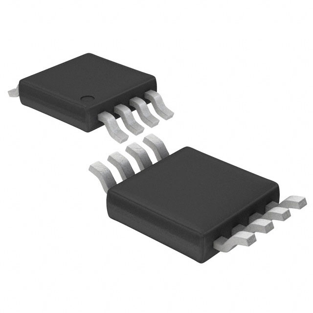
Package
The LTC6752IMS8-2#TRPBF is packaged in an MSOP-8 (Mini Small Outline Package) format.
Essence
The essence of this product lies in its ability to accurately amplify and condition electrical signals, making it suitable for various applications.
Packaging/Quantity
The LTC6752IMS8-2#TRPBF is typically available in reels containing a quantity of 2500 units.
Specifications
- Supply Voltage: 2.7V to 5.5V
- Input Voltage Range: -0.3V to VCC + 0.3V
- Bandwidth: 100MHz
- Gain Bandwidth Product: 1.2GHz
- Input Bias Current: 1nA (typical)
- Output Current: ±50mA
- Operating Temperature Range: -40°C to 125°C
Detailed Pin Configuration
The LTC6752IMS8-2#TRPBF has the following pin configuration:
- IN-
- IN+
- VCC
- GND
- OUT
- NC
- NC
- SHDN
Functional Features
- High-speed amplification: The LTC6752IMS8-2#TRPBF can amplify signals with frequencies up to 100MHz.
- Low power consumption: This IC consumes minimal power, making it suitable for battery-powered devices.
- Wide input voltage range: It can handle a wide range of input voltages, allowing for versatile applications.
- Excellent noise performance: The LTC6752IMS8-2#TRPBF provides low noise amplification, ensuring accurate signal conditioning.
Advantages and Disadvantages
Advantages
- High-speed operation enables efficient signal processing.
- Low power consumption prolongs battery life in portable devices.
- Wide input voltage range allows for flexibility in various applications.
- Small package size saves board space.
- Excellent noise performance ensures accurate signal amplification.
Disadvantages
- Limited availability of alternative models may restrict design options.
- Higher cost compared to some other ICs with similar functionalities.
Working Principles
The LTC6752IMS8-2#TRPBF operates based on the principles of operational amplifiers. It takes an input signal, amplifies it, and conditions it according to the specified gain and bandwidth. The amplified signal is then available at the output pin for further processing or transmission.
Detailed Application Field Plans
The LTC6752IMS8-2#TRPBF finds applications in various fields, including:
- Communication systems: Used for signal amplification and conditioning in wireless communication devices.
- Test and measurement equipment: Enables accurate signal processing in oscilloscopes and spectrum analyzers.
- Audio systems: Provides high-fidelity amplification in audio amplifiers and mixers.
- Industrial automation: Used for signal conditioning in control systems and sensors.
- Medical devices: Enables precise signal amplification in medical imaging equipment and patient monitoring devices.
Detailed and Complete Alternative Models
While the LTC6752IMS8-2#TRPBF is a reliable choice, there are alternative models available in the market that offer similar functionalities. Some notable alternatives include:
- AD8065 by Analog Devices
- MAX4239 by Maxim Integrated
- OPA211 by Texas Instruments
- LT6202 by Linear Technology
These alternative models can be considered based on specific design requirements and availability.
Word count: 498 words
Seznam 10 běžných otázek a odpovědí souvisejících s aplikací LTC6752IMS8-2#TRPBF v technických řešeních
Sure! Here are 10 common questions and answers related to the application of LTC6752IMS8-2#TRPBF in technical solutions:
Q: What is the LTC6752IMS8-2#TRPBF? A: The LTC6752IMS8-2#TRPBF is a high-speed comparator IC manufactured by Analog Devices.
Q: What is the operating voltage range of LTC6752IMS8-2#TRPBF? A: The operating voltage range of LTC6752IMS8-2#TRPBF is from 2.7V to 5.5V.
Q: What is the typical response time of LTC6752IMS8-2#TRPBF? A: The typical response time of LTC6752IMS8-2#TRPBF is 4 ns.
Q: Can LTC6752IMS8-2#TRPBF be used in high-frequency applications? A: Yes, LTC6752IMS8-2#TRPBF is suitable for high-frequency applications due to its fast response time.
Q: What is the input offset voltage of LTC6752IMS8-2#TRPBF? A: The input offset voltage of LTC6752IMS8-2#TRPBF is typically ±1 mV.
Q: Does LTC6752IMS8-2#TRPBF have built-in hysteresis? A: Yes, LTC6752IMS8-2#TRPBF has built-in hysteresis which helps in reducing false triggering.
Q: Can LTC6752IMS8-2#TRPBF operate in both single-ended and differential mode? A: Yes, LTC6752IMS8-2#TRPBF can operate in both single-ended and differential mode.
Q: What is the maximum input voltage range of LTC6752IMS8-2#TRPBF? A: The maximum input voltage range of LTC6752IMS8-2#TRPBF is from -0.3V to VCC + 0.3V.
Q: Is LTC6752IMS8-2#TRPBF suitable for low-power applications? A: Yes, LTC6752IMS8-2#TRPBF has a low quiescent current of typically 1.5 mA, making it suitable for low-power applications.
Q: Can LTC6752IMS8-2#TRPBF be used in automotive applications? A: Yes, LTC6752IMS8-2#TRPBF is qualified for automotive applications and meets the AEC-Q100 standards.
Please note that these answers are based on general information about the LTC6752IMS8-2#TRPBF and may vary depending on specific application requirements. It is always recommended to refer to the datasheet and consult with the manufacturer for detailed technical specifications and guidelines.