

Viz Specifikace pro podrobnosti o produktu.
LTC7541AJSW#PBF
Product Overview
Category
LTC7541AJSW#PBF belongs to the category of digital-to-analog converters (DACs).
Use
This product is used to convert digital signals into analog signals, making it suitable for various applications such as audio systems, instrumentation, and communication devices.
Characteristics
- High precision: LTC7541AJSW#PBF offers exceptional accuracy in converting digital data to analog signals.
- Low power consumption: This DAC operates efficiently with minimal power requirements.
- Wide voltage range: It supports a wide range of input voltages, allowing flexibility in different applications.
- Fast conversion speed: The LTC7541AJSW#PBF provides rapid conversion of digital signals to analog outputs.
Package
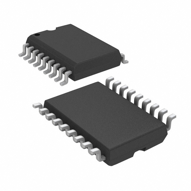
LTC7541AJSW#PBF comes in a small outline package (SOIC) which ensures easy integration into circuit boards.
Essence
The essence of LTC7541AJSW#PBF lies in its ability to accurately convert digital data into analog signals, enabling precise control and manipulation of analog systems.
Packaging/Quantity
This product is typically packaged in reels or tubes, with each reel containing a specific quantity of LTC7541AJSW#PBF units. The exact quantity may vary depending on the manufacturer's specifications.
Specifications
- Resolution: 12 bits
- Supply Voltage: 2.7V to 5.5V
- Operating Temperature Range: -40°C to 85°C
- Output Voltage Range: 0V to Vref
- DNL (Differential Non-Linearity): ±0.5 LSB (max)
- INL (Integral Non-Linearity): ±1 LSB (max)
Detailed Pin Configuration
The LTC7541AJSW#PBF has the following pin configuration:
- VDD: Power supply voltage
- VREF: Reference voltage input
- AGND: Analog ground
- OUT: Analog output
- DIN0-DIN11: Digital input pins (12-bit data)
- CS: Chip select input
- SCLK: Serial clock input
- GND: Ground
Functional Features
- High accuracy conversion: LTC7541AJSW#PBF ensures precise conversion of digital signals to analog outputs.
- Serial interface: It supports a serial interface for easy integration with microcontrollers and other digital systems.
- Power-down mode: This DAC offers a power-down mode to conserve energy when not in use.
- Low glitch energy: The LTC7541AJSW#PBF minimizes glitches during transitions, ensuring smooth analog signal generation.
Advantages and Disadvantages
Advantages
- High precision conversion
- Low power consumption
- Wide voltage range
- Fast conversion speed
- Small package size for easy integration
Disadvantages
- Limited resolution compared to higher-end DACs
- May require additional external components for certain applications
Working Principles
LTC7541AJSW#PBF operates on the principle of converting binary digital data into corresponding analog voltages. It utilizes an internal digital-to-analog conversion algorithm to accurately translate the digital input into an analog output voltage. The converted analog signal can then be used to control various analog systems or devices.
Detailed Application Field Plans
The LTC7541AJSW#PBF finds application in various fields, including:
- Audio Systems: It can be used in audio equipment such as amplifiers, mixers, and digital audio workstations to convert digital audio signals into analog outputs.
- Instrumentation: This DAC is suitable for precision measurement instruments where accurate analog control signals are required.
- Communication Devices: LTC7541AJSW#PBF can be used in communication devices like modems and routers to convert digital control signals into analog voltages for signal modulation.
Detailed and Complete Alternative Models
- LTC7540AJSW#PBF: Similar to LTC7541AJSW#PBF, but with 10-bit resolution.
- LTC7542AJSW#PBF: Similar to LTC7541AJSW#PBF, but with 14-bit resolution.
- MAX5216CPA+: An alternative DAC with similar characteristics and package, offering 16-bit resolution.
These alternative models provide options with varying resolutions to suit different application requirements.
Word count: 511 words
Seznam 10 běžných otázek a odpovědí souvisejících s aplikací LTC7541AJSW#PBF v technických řešeních
Sure! Here are 10 common questions and answers related to the application of LTC7541AJSW#PBF in technical solutions:
Q1: What is LTC7541AJSW#PBF? A1: LTC7541AJSW#PBF is a specific model number for a digital-to-analog converter (DAC) chip manufactured by Linear Technology Corporation.
Q2: What is the purpose of LTC7541AJSW#PBF? A2: The LTC7541AJSW#PBF is designed to convert digital signals into analog voltages, making it useful in various applications such as instrumentation, control systems, and communication devices.
Q3: What is the resolution of LTC7541AJSW#PBF? A3: The LTC7541AJSW#PBF has a resolution of 12 bits, meaning it can represent analog voltages with 4096 discrete levels.
Q4: What is the operating voltage range of LTC7541AJSW#PBF? A4: The LTC7541AJSW#PBF operates from a single power supply voltage ranging from 2.7V to 5.5V.
Q5: What is the output voltage range of LTC7541AJSW#PBF? A5: The output voltage range of LTC7541AJSW#PBF is programmable and can be set between 0V and the reference voltage applied to the chip.
Q6: How does LTC7541AJSW#PBF communicate with a microcontroller or other digital devices? A6: LTC7541AJSW#PBF uses a serial interface called SPI (Serial Peripheral Interface) to receive digital data from a microcontroller or other digital devices.
Q7: Can LTC7541AJSW#PBF be used in both single-ended and differential output configurations? A7: Yes, LTC7541AJSW#PBF can be configured for both single-ended and differential output modes, providing flexibility in various applications.
Q8: What is the settling time of LTC7541AJSW#PBF? A8: The settling time of LTC7541AJSW#PBF is typically 3.5µs, which refers to the time it takes for the output voltage to stabilize after a digital input change.
Q9: Does LTC7541AJSW#PBF have any built-in reference voltage? A9: No, LTC7541AJSW#PBF requires an external reference voltage to determine its output voltage range.
Q10: Is LTC7541AJSW#PBF available in different package options? A10: Yes, LTC7541AJSW#PBF is available in a small 20-pin wide SOIC (Small Outline Integrated Circuit) package.
Please note that these answers are general and may vary depending on the specific application and requirements. It's always recommended to refer to the datasheet and consult with the manufacturer for detailed information.